- 您现在的位置:买卖IC网 > PDF目录97909 > EM6617DL24A Advanced Synchronous Rectified Buck MOSFET Drivers with Pre-POR OVP; Temperature Range: 0°C to 70°C; Package: 8-SOIC PDF资料下载
参数资料
| 型号: | EM6617DL24A |
| 英文描述: | Advanced Synchronous Rectified Buck MOSFET Drivers with Pre-POR OVP; Temperature Range: 0°C to 70°C; Package: 8-SOIC |
| 中文描述: | 微控制器 |
| 文件页数: | 30/67页 |
| 文件大小: | 824K |
| 代理商: | EM6617DL24A |
第1页第2页第3页第4页第5页第6页第7页第8页第9页第10页第11页第12页第13页第14页第15页第16页第17页第18页第19页第20页第21页第22页第23页第24页第25页第26页第27页第28页第29页当前第30页第31页第32页第33页第34页第35页第36页第37页第38页第39页第40页第41页第42页第43页第44页第45页第46页第47页第48页第49页第50页第51页第52页第53页第54页第55页第56页第57页第58页第59页第60页第61页第62页第63页第64页第65页第66页第67页
EM6617
03/02 REV. C/442
Copyright
2002, EM Microelectronic-Marin SA
36
www.emmicroelectronic.com
11. EEPROM ( 64
×××× 8 Bit )
The EEPROM addressing is indirect using 6 bits (64 addresses) defined in RegEEPAdr and RegEEPCntl
registers. The EEPROM consist of 2 pages 32x8bit each, address EEPAdr[4 :0]. The page is selected in the
RegEEPCntl
register bit EEPage. So the user can address the EEPROM as it would be one block of 64x8 bit.
Any access to the EEPROM is done in two phases. 1
st, one needs to define the address location. 2nd, one
needs to start the desired action, read or write. Refer to the examples below..
How to read data from EEPROM :
1
st inst.
: write EEPROM address (4 low bits) in RegEEPAddr register.
2
nd inst.
: write the high address bit, page and select reading operation in RegEEPCntl.
(EEPAdr[4], EEPage, EEPRdWr=0)
3
rd inst.
: NOP instruction in case of 128kHz operation (metal option setting).
4
th inst.
: read EEPROM low data in RegEEPDataL register.
5
th inst.
: read EEPROM high data in RegEEPDataH register.
The two last instructions can be executed in the reverse order.
How to write data in EEPROM :
1
st inst.
: write EEPROM address (4 low bits) in RegEEPAdr register.
2
nd inst.
: write EEPROM low data in RegEEPDataL register.
3
rd inst.: write EEPROM high data in RegEEPDataH register.
4
th inst.
: write the high address bit, page and select writing operation in RegEEPCntl.
(EEPAdr[4], EEPage, EEPRdWr=1)
5
th .
: IRQEEP is generated at the end of write.
The three first instructions can be executed in any order.
Writing RegEEPCntl register starts automatically EEPROM reading or writing operation according to the bit
EEPRdWr
.
EEPROM access time is max. 20s : Data is
available in RegEEPDataL and RegEEPDataH
registers at the instruction following the read
access on 32kHz system clock The read signal is
1.5 system clock wide. The CPU reads at end of
phase 3.
With the 128kHz metal option the EERead signal
is 3.5 system clock cycles wide. Using this option
the user must use a NOP instruction before
actually reading the RegEEPDataL,H values.
EEPROM writing operation lasts 24ms (Erase followed by write). The flag EEPBusy in RegEEPCntl register
stays high until the writing operation is finished. An interrupt request IRQEEP is generated at the end of each
writing operation. While EEPBusy is high the EEPROM must not be used at all. The EEPROM interrupt request
can be masked (default) (MaskIRQEEP bit). See also the interrupt handling section 13 for further information .
Note : Any Reset or sleep mode will immediately cancel the EEPROM write operation.
The data to be stored at this time may be corrupted.
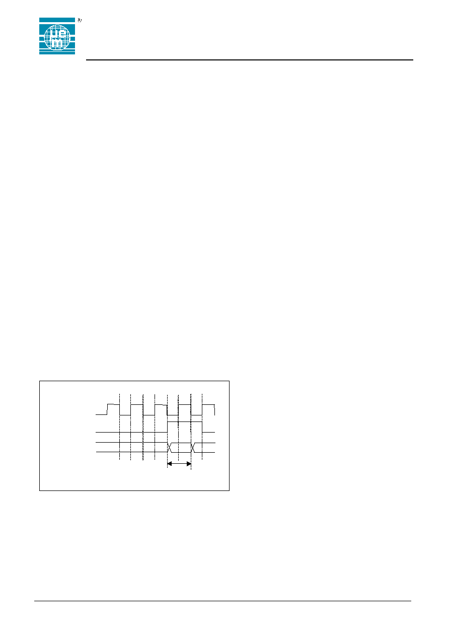
Figure 27. Read Timing 32kHz operation
Max. 20
s
EE Read
EE Stable Data
Sys. Clock
CPU Phase
4
3
2
1
4
3
1 2
相关PDF资料 |
PDF描述 |
|---|---|
| EM6617DL28A | Advanced Synchronous Rectified Buck MOSFET Drivers with Pre-POR OVP; Temperature Range: 0°C to 70°C; Package: 8-SOIC T&R |
| EM6617SO24A | 30V N-Channel PowerTrench MOSFET |
| EM6617SO24B | 30V N-Channel PowerTrench MOSFET |
| EM6617SO28A | Advanced Synchronous Rectified Buck MOSFET Drivers with Pre-POR OVP; Temperature Range: 0°C to 70°C; Package: 8-EPSOIC T&R |
| EM6617SO28B | Advanced Synchronous Rectified Buck MOSFET Drivers with Pre-POR OVP; Temperature Range: -40°C to 85°C; Package: 8-EPSOIC T&R |
相关代理商/技术参数 |
参数描述 |
|---|---|
| EM6617DL28A | 制造商:未知厂家 制造商全称:未知厂家 功能描述:Microcontroller |
| EM6617SO24A | 制造商:未知厂家 制造商全称:未知厂家 功能描述:Microcontroller |
| EM6617SO24B | 制造商:未知厂家 制造商全称:未知厂家 功能描述:Microcontroller |
| EM6617SO28A | 制造商:未知厂家 制造商全称:未知厂家 功能描述:Microcontroller |
| EM6617SO28B | 制造商:未知厂家 制造商全称:未知厂家 功能描述:Microcontroller |
发布紧急采购,3分钟左右您将得到回复。