- 您现在的位置:买卖IC网 > PDF目录295883 > EN29LV320B-70TIP (Eon Silicon Solution Inc.) 32 Megabit (4096K x 8-bit / 2048K x 16-bit) Flash Memory Boot Sector Flash Memory, CMOS 3.0 Volt-only PDF资料下载
参数资料
| 型号: | EN29LV320B-70TIP |
| 厂商: | Eon Silicon Solution Inc. |
| 英文描述: | 32 Megabit (4096K x 8-bit / 2048K x 16-bit) Flash Memory Boot Sector Flash Memory, CMOS 3.0 Volt-only |
| 中文描述: | 32兆位(4096K × 8位/ 2048K x 16位)闪存引导扇区闪存,CMOS 3.0伏,只 |
| 文件页数: | 8/49页 |
| 文件大小: | 437K |
| 代理商: | EN29LV320B-70TIP |
第1页第2页第3页第4页第5页第6页第7页当前第8页第9页第10页第11页第12页第13页第14页第15页第16页第17页第18页第19页第20页第21页第22页第23页第24页第25页第26页第27页第28页第29页第30页第31页第32页第33页第34页第35页第36页第37页第38页第39页第40页第41页第42页第43页第44页第45页第46页第47页第48页第49页
This Data Sheet may be revised by subsequent versions
2004 Eon Silicon Solution, Inc., www.essi.com.tw
or modifications due to changes in technical specifications.
16
EN29LV320
Rev. E, Issue Date: 2006/05/16
This device enters the CFI Query mode when the system writes the CFI Query command, 98h, to
address 55h in word mode (or address AAh in byte mode), any time the device is ready to read
array data.
The system can read CFI information at the addresses given in Tables 5-8.In word mode, the upper
address bits (A7–MSB) must be all zeros. To terminate reading CFI data, the system must write the
reset command.
The system can also write the CFI query command when the device is in the autoselect mode. The
device enters the CFI query mode and the system can read CFI data at the addresses given in
Tables 5–8. The system must write the reset command to return the device to the autoselect mode.
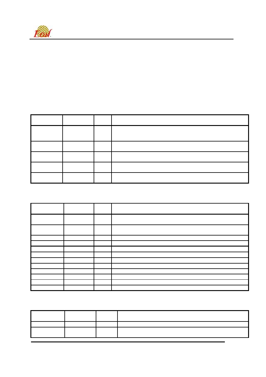
Table 5. CFI Query Identification String
Addresses
(Word Mode)
Adresses
(Byte Mode)
Data
Description
10h
11h
12h
20h
22h
24h
0051h
0052h
0059h
Query Unique ASCII string “QRY”
13h
14h
26h
28h
0002h
0000h
Primary OEM Command Set
15h
16h
2Ah
2Ch
0040h
0000h
Address for Primary Extended Table
17h
18h
2Eh
30h
0000h
Alternate OEM Command set (00h = none exists)
19h
1Ah
32h
34h
0000h
Address for Alternate OEM Extended Table (00h = none exists)
Table 6. System Interface String
Addresses
(Word Mode)
Addresses
(Byte Mode)
Data
Description
1Bh
36h
0027h
Vcc Min (write/erase)
DQ7-DQ4: volt, DQ3 –DQ0: 100 millivolt
1Ch
38h
0036h
Vcc Max (write/erase)
DQ7-DQ4: volt, DQ3 –DQ0: 100 millivolt
1Dh
3Ah
0000h
Vpp Min. voltage (00h = no Vpp pin present)
1Eh
3Ch
0000h
Vpp Max. voltage (00h = no Vpp pin present)
1Fh
3Eh
0004h
Typical timeout per single byte/word write 2
P
N
P
S
20h
40h
0000h
Typical timeout for Min, size buffer write 2
P
N
P
S (00h = not supported)
21h
42h
000Ah
Typical timeout per individual block erase 2
P
N
P
ms
22h
44h
0000h
Typical timeout for full chip erase 2
P
N
P
ms (00h = not supported)
23h
46h
0005h
Max. timeout for byte/word write 2
P
N
P
times typical
24h
48h
0000h
Max. timeout for buffer write 2
P
N
P
times typical
25h
4Ah
0004h
Max. timeout per individual block erase 2
P
N
P
times typical
26h
4Ch
0000h
Max timeout for full chip erase 2
P
N
P
times typical (00h = not supported)
Table 7. Device Geometry Definition
Addresses
(Word mode)
Addresses
(Byte Mode)
Data
Description
27h
4Eh
0016h
Device Size = 2
P
N
P
bytes
28h
29h
50h
52h
0002h
0000h
Flash Device Interface description (refer to CFI publication 100)
相关PDF资料 |
PDF描述 |
|---|---|
| EN29LV320B-70TI | 32 Megabit (4096K x 8-bit / 2048K x 16-bit) Flash Memory Boot Sector Flash Memory, CMOS 3.0 Volt-only |
| EN29LV320B-90BCP | 32 Megabit (4096K x 8-bit / 2048K x 16-bit) Flash Memory Boot Sector Flash Memory, CMOS 3.0 Volt-only |
| EN29LV320B-90BC | 32 Megabit (4096K x 8-bit / 2048K x 16-bit) Flash Memory Boot Sector Flash Memory, CMOS 3.0 Volt-only |
| EN29LV320B-90BIP | 32 Megabit (4096K x 8-bit / 2048K x 16-bit) Flash Memory Boot Sector Flash Memory, CMOS 3.0 Volt-only |
| EN29LV320B-90BI | 32 Megabit (4096K x 8-bit / 2048K x 16-bit) Flash Memory Boot Sector Flash Memory, CMOS 3.0 Volt-only |
相关代理商/技术参数 |
参数描述 |
|---|---|
| EN29LV320BT-70TIP | 制造商:EON SILICON SOLUTION INC 功能描述:32M TOP BOOT TSOP |
| EN29LV320CT-70TIP | 制造商:EON SILICON SOLUTION INC 功能描述:32M Parallel Flash, x8/x16, 70ns, TSOP48 |
| EN29LV400AB-70TCP | 制造商:EON SILICON SOLUTION INC 功能描述:EN29LV400A Series, 4 Mbit (512 K x 8) 70 NS 48 TSOP 3 V Bottom Boot NOR Flash |
| EN29LV400AB-70TIP | 制造商:EON SILICON SOLUTION INC 功能描述:EN29LV400A Series 4 Mbit (512 K x 8) 70 NS 48 TSOP 3 V Bottom Boot NOR Flash |
| EN29LV400AT-70TCP | 制造商:EON SILICON SOLUTION INC 功能描述:4 Mb PAR NOR 512Kx8bit/256Kx16bit 3V 48-TSOP |
发布紧急采购,3分钟左右您将得到回复。