- 您现在的位置:买卖IC网 > PDF目录295883 > EN29LV320B-90BI (Eon Silicon Solution Inc.) 32 Megabit (4096K x 8-bit / 2048K x 16-bit) Flash Memory Boot Sector Flash Memory, CMOS 3.0 Volt-only PDF资料下载
参数资料
| 型号: | EN29LV320B-90BI |
| 厂商: | Eon Silicon Solution Inc. |
| 英文描述: | 32 Megabit (4096K x 8-bit / 2048K x 16-bit) Flash Memory Boot Sector Flash Memory, CMOS 3.0 Volt-only |
| 中文描述: | 32兆位(4096K × 8位/ 2048K x 16位)闪存引导扇区闪存,CMOS 3.0伏,只 |
| 文件页数: | 11/49页 |
| 文件大小: | 437K |
| 代理商: | EN29LV320B-90BI |
第1页第2页第3页第4页第5页第6页第7页第8页第9页第10页当前第11页第12页第13页第14页第15页第16页第17页第18页第19页第20页第21页第22页第23页第24页第25页第26页第27页第28页第29页第30页第31页第32页第33页第34页第35页第36页第37页第38页第39页第40页第41页第42页第43页第44页第45页第46页第47页第48页第49页
This Data Sheet may be revised by subsequent versions
2004 Eon Silicon Solution, Inc., www.essi.com.tw
or modifications due to changes in technical specifications.
19
EN29LV320
Rev. E, Issue Date: 2006/05/16
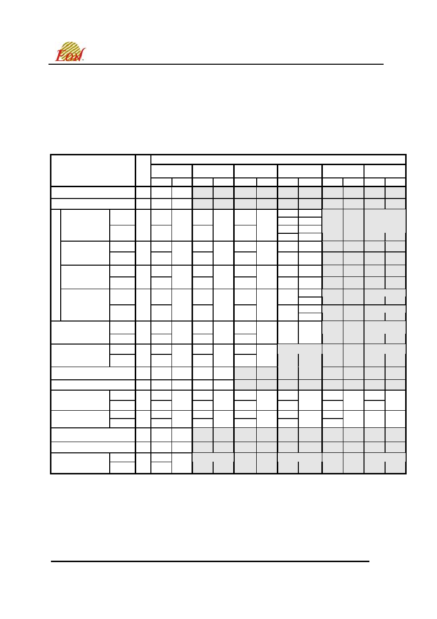
COMMAND DEFINITIONS
The operations of the device are selected by one or more commands written into the command
register. Commands are made up of data sequences written at specific addresses via the
command register. The sequences for the specified operation are defined in the Command
Definitions table (Table 9). Incorrect addresses, incorrect data values or improper sequences will
reset the device to Read Mode.
Table 9. EN29LV320 Command Definitions
Bus Cycles
1
P
st
P
Cycle
2
P
nd
P
Cycle
3
P
rd
P
Cycle
4
P
th
P
Cycle
5
P
th
P
Cycle
6
P
th
P
Cycle
Command
Sequence
Cycles
Read
1
RA
RD
Reset
1
xxx
F0
000
7F
Word
555
2AA
555
100
1C
000
7F
Manufacturer
ID
Byte
4
AAA
AA
555
55
AAA
90
200
1C
Word
555
2AA
555
x01
22F6
Device ID
Top Boot
Byte
4
AAA
AA
555
55
AAA
90
x02
F6
Word
555
2AA
555
x01
22F9
Device ID
Bottom Boot
Byte
4
AAA
AA
555
55
AAA
90
x02
F9
00
Word
555
2AA
555
(SA)
X02
01
00
Autoselect
Sector Protect
Verify
Byte
4
AAA
AA
555
55
AAA
90
(SA)
X04
01
Word
555
2AA
555
Program
Byte
4
AAA
AA
555
55
AAA
A0
PA
PD
Word
555
2AA
555
Unlock Bypass
Byte
3
AAA
AA
555
55
AAA
20
Unlock Bypass Program
2
XXX
A0
PA
PD
Unlock Bypass Reset
2
XXX
90
XXX
00
Word
555
2AA
555
2AA
555
Chip Erase
Byte
6
AAA
AA
555
55
AAA
80
AAA
AA
555
55
AAA
10
Word
555
2AA
555
2AA
Sector Erase
Byte
6
AAA
AA
555
55
AAA
80
AAA
AA
555
55
SA
30
Sector Erase Suspend
1
xxx
B0
Sector Erase Resume
1
xxx
30
Word
55
CFI Query
Byte
1
AA
98
Address and Data values indicated are in hex. Unless specified, all bus cycles are write cycles
RA = Read Address: address of the memory location to be read. This is a read cycle.
RD = Read Data: data read from location RA during Read operation. This is a read cycle.
PA = Program Address: address of the memory location to be programmed. X = Don’t-Care
PD = Program Data: data to be programmed at location PA
SA = Sector Address: address of the Sector to be erased or verified. Address bits A20-A12 uniquely select any Sector.
相关PDF资料 |
PDF描述 |
|---|---|
| EN29LV320B-90TC | 32 Megabit (4096K x 8-bit / 2048K x 16-bit) Flash Memory Boot Sector Flash Memory, CMOS 3.0 Volt-only |
| EN3 | GLASS FILLED POLYETHYLENE POLYMER, FEMALE; MALE, CIRCULAR CONNECTOR, CRIMP; SOLDER |
| EN3I2F16PAGK | 2 CONTACT(S), FEMALE, CIRCULAR CONNECTOR |
| EN3I2F16PAG | 2 CONTACT(S), FEMALE, CIRCULAR CONNECTOR |
| EN3I2F16PK | 2 CONTACT(S), FEMALE, CIRCULAR CONNECTOR |
相关代理商/技术参数 |
参数描述 |
|---|---|
| EN29LV320BT-70TIP | 制造商:EON SILICON SOLUTION INC 功能描述:32M TOP BOOT TSOP |
| EN29LV320CT-70TIP | 制造商:EON SILICON SOLUTION INC 功能描述:32M Parallel Flash, x8/x16, 70ns, TSOP48 |
| EN29LV400AB-70TCP | 制造商:EON SILICON SOLUTION INC 功能描述:EN29LV400A Series, 4 Mbit (512 K x 8) 70 NS 48 TSOP 3 V Bottom Boot NOR Flash |
| EN29LV400AB-70TIP | 制造商:EON SILICON SOLUTION INC 功能描述:EN29LV400A Series 4 Mbit (512 K x 8) 70 NS 48 TSOP 3 V Bottom Boot NOR Flash |
| EN29LV400AT-70TCP | 制造商:EON SILICON SOLUTION INC 功能描述:4 Mb PAR NOR 512Kx8bit/256Kx16bit 3V 48-TSOP |
发布紧急采购,3分钟左右您将得到回复。