- 您现在的位置:买卖IC网 > PDF目录362734 > EP1C6F100I8ES (Altera Corporation) Cyclone FPGA Family Data Sheet PDF资料下载
参数资料
| 型号: | EP1C6F100I8ES |
| 厂商: | Altera Corporation |
| 英文描述: | Cyclone FPGA Family Data Sheet |
| 中文描述: | 气旋的FPGA系列数据手册 |
| 文件页数: | 14/104页 |
| 文件大小: | 763K |
| 代理商: | EP1C6F100I8ES |
第1页第2页第3页第4页第5页第6页第7页第8页第9页第10页第11页第12页第13页当前第14页第15页第16页第17页第18页第19页第20页第21页第22页第23页第24页第25页第26页第27页第28页第29页第30页第31页第32页第33页第34页第35页第36页第37页第38页第39页第40页第41页第42页第43页第44页第45页第46页第47页第48页第49页第50页第51页第52页第53页第54页第55页第56页第57页第58页第59页第60页第61页第62页第63页第64页第65页第66页第67页第68页第69页第70页第71页第72页第73页第74页第75页第76页第77页第78页第79页第80页第81页第82页第83页第84页第85页第86页第87页第88页第89页第90页第91页第92页第93页第94页第95页第96页第97页第98页第99页第100页第101页第102页第103页第104页
2–8
Preliminary
Altera Corporation
January 2007
Cyclone Device Handbook, Volume 1
preset/load, synchronous clear, synchronous load, and clock enable
control for the register. These LAB-wide signals are available in all LE
modes. The
addnsub
control signal is allowed in arithmetic mode.
The Quartus II software, in conjunction with parameterized functions
such as library of parameterized modules (LPM) functions, automatically
chooses the appropriate mode for common functions such as counters,
adders, subtractors, and arithmetic functions. If required, you can also
create special-purpose functions that specify which LE operating mode to
use for optimal performance.
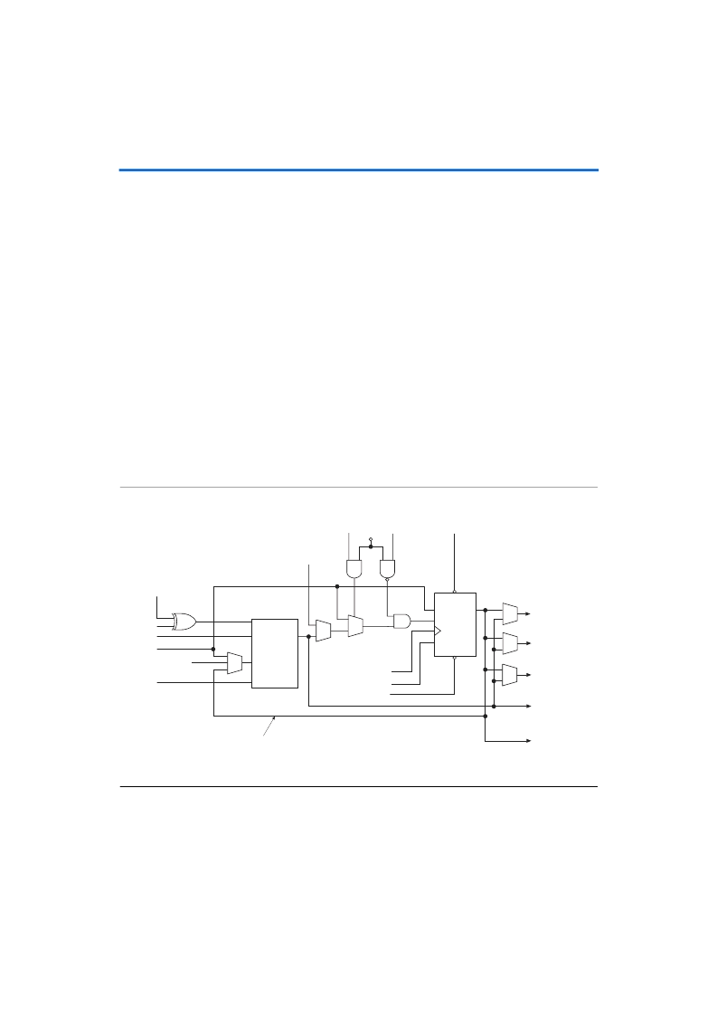
Normal Mode
The normal mode is suitable for general logic applications and
combinatorial functions. In normal mode, four data inputs from the LAB
local interconnect are inputs to a four-input LUT (see
Figure 2–6
). The
Quartus II Compiler automatically selects the carry-in or the
data3
signal as one of the inputs to the LUT. Each LE can use LUT chain
connections to drive its combinatorial output directly to the next LE in the
LAB. Asynchronous load data for the register comes from the
data3
input of the LE. LEs in normal mode support packed registers.
Figure 2–6. LE in Normal Mode
Note to
Figure 2–6
:
(1)
This signal is only allowed in normal mode if the LE is at the end of an adder/subtractor chain.
data1
data2
data3
cin (from cout
of previous LE)
4-Input
LUT
data4
addnsub (LAB Wide)
clock (LAB Wide)
ena (LAB Wide)
aclr (LAB Wide)
aload
(LAB Wide)
ALD/PRE
ADATA
CLRN
D
Q
ENA
sclear
(LAB Wide)
sload
(LAB Wide)
Register chain
connection
LUT chain
connection
Register
chain output
Row, column, and
direct link routing
Row, column, and
direct link routing
Local routing
Register Feedback
(1)
相关PDF资料 |
PDF描述 |
|---|---|
| EP1C6F144C6ES | Cyclone FPGA Family Data Sheet |
| EP1C6F144C7ES | Cyclone FPGA Family Data Sheet |
| EP1C6F144C8ES | Cyclone FPGA Family Data Sheet |
| EP1C6F144I6ES | Cyclone FPGA Family Data Sheet |
| EP1C6F144I7ES | Cyclone FPGA Family Data Sheet |
相关代理商/技术参数 |
参数描述 |
|---|---|
| EP1C6F256C6 | 功能描述:FPGA - 现场可编程门阵列 FPGA - Cyclone I 598 LABs 185 IOs RoHS:否 制造商:Altera Corporation 系列:Cyclone V E 栅极数量: 逻辑块数量:943 内嵌式块RAM - EBR:1956 kbit 输入/输出端数量:128 最大工作频率:800 MHz 工作电源电压:1.1 V 最大工作温度:+ 70 C 安装风格:SMD/SMT 封装 / 箱体:FBGA-256 |
| EP1C6F256C6N | 功能描述:FPGA - 现场可编程门阵列 FPGA - Cyclone I 598 LABs 185 IOs RoHS:否 制造商:Altera Corporation 系列:Cyclone V E 栅极数量: 逻辑块数量:943 内嵌式块RAM - EBR:1956 kbit 输入/输出端数量:128 最大工作频率:800 MHz 工作电源电压:1.1 V 最大工作温度:+ 70 C 安装风格:SMD/SMT 封装 / 箱体:FBGA-256 |
| EP1C6F256C7 | 功能描述:FPGA - 现场可编程门阵列 FPGA - Cyclone I 598 LABs 185 IOs RoHS:否 制造商:Altera Corporation 系列:Cyclone V E 栅极数量: 逻辑块数量:943 内嵌式块RAM - EBR:1956 kbit 输入/输出端数量:128 最大工作频率:800 MHz 工作电源电压:1.1 V 最大工作温度:+ 70 C 安装风格:SMD/SMT 封装 / 箱体:FBGA-256 |
| EP1C6F256C7N | 功能描述:FPGA - 现场可编程门阵列 FPGA - Cyclone I 598 LABs 185 IOs RoHS:否 制造商:Altera Corporation 系列:Cyclone V E 栅极数量: 逻辑块数量:943 内嵌式块RAM - EBR:1956 kbit 输入/输出端数量:128 最大工作频率:800 MHz 工作电源电压:1.1 V 最大工作温度:+ 70 C 安装风格:SMD/SMT 封装 / 箱体:FBGA-256 |
| EP1C6F256C8 | 功能描述:FPGA - 现场可编程门阵列 FPGA - Cyclone I 598 LABs 185 IOs RoHS:否 制造商:Altera Corporation 系列:Cyclone V E 栅极数量: 逻辑块数量:943 内嵌式块RAM - EBR:1956 kbit 输入/输出端数量:128 最大工作频率:800 MHz 工作电源电压:1.1 V 最大工作温度:+ 70 C 安装风格:SMD/SMT 封装 / 箱体:FBGA-256 |
发布紧急采购,3分钟左右您将得到回复。