参数资料
| 型号: | EP1K100QC208-2 |
| 厂商: | Altera |
| 文件页数: | 55/86页 |
| 文件大小: | 0K |
| 描述: | IC ACEX 1K FPGA 100K 208-PQFP |
| 产品培训模块: | Three Reasons to Use FPGA's in Industrial Designs |
| 标准包装: | 144 |
| 系列: | ACEX-1K® |
| LAB/CLB数: | 624 |
| 逻辑元件/单元数: | 4992 |
| RAM 位总计: | 49152 |
| 输入/输出数: | 147 |
| 门数: | 257000 |
| 电源电压: | 2.375 V ~ 2.625 V |
| 安装类型: | 表面贴装 |
| 工作温度: | 0°C ~ 70°C |
| 封装/外壳: | 208-BFQFP |
| 供应商设备封装: | 208-PQFP(28x28) |
| 其它名称: | 544-1001 |
第1页第2页第3页第4页第5页第6页第7页第8页第9页第10页第11页第12页第13页第14页第15页第16页第17页第18页第19页第20页第21页第22页第23页第24页第25页第26页第27页第28页第29页第30页第31页第32页第33页第34页第35页第36页第37页第38页第39页第40页第41页第42页第43页第44页第45页第46页第47页第48页第49页第50页第51页第52页第53页第54页当前第55页第56页第57页第58页第59页第60页第61页第62页第63页第64页第65页第66页第67页第68页第69页第70页第71页第72页第73页第74页第75页第76页第77页第78页第79页第80页第81页第82页第83页第84页第85页第86页
Altera Corporation
59
ACEX 1K Programmable Logic Device Family Data Sheet
D
e
ve
lo
pm
e
n
t
13
To
o
ls
and their symbols.
Notes to tables:
(1)
External reference timing parameters are factory-tested, worst-case values specified by Altera. A representative
subset of signal paths is tested to approximate typical device applications.
(2)
Contact Altera Applications for test circuit specifications and test conditions.
(3)
These timing parameters are sample-tested only.
(4)
This parameter is measured with the measurement and test conditions, including load, specified in the PCI Local
Bus Specification, Revision 2.2.
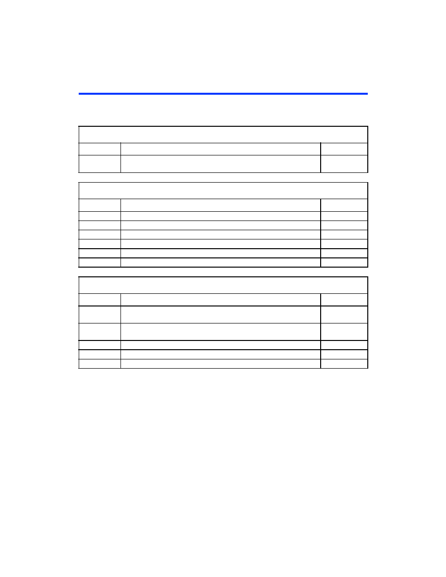
Table 27. External Reference Timing Parameters
Symbol
Parameter
Conditions
tDRR
Register-to-register delay via four LEs, three row interconnects, and four local
interconnects
Table 28. External Timing Parameters
Symbol
Parameter
Conditions
tINSU
Setup time with global clock at IOE register
tINH
Hold time with global clock at IOE register
tOUTCO
Clock-to-output delay with global clock at IOE register
tPCISU
Setup time with global clock for registers used in PCI designs
tPCIH
Hold time with global clock for registers used in PCI designs
tPCICO
Clock-to-output delay with global clock for registers used in PCI designs
Table 29. External Bidirectional Timing Parameters
Symbol
Parameter
Conditions
tINSUBIDIR
Setup time for bidirectional pins with global clock at same-row or same-
column LE register
tINHBIDIR
Hold time for bidirectional pins with global clock at same-row or same-column
LE register
tOUTCOBIDIR
Clock-to-output delay for bidirectional pins with global clock at IOE register
CI = 35 pF
tXZBIDIR
Synchronous IOE output buffer disable delay
CI = 35 pF
tZXBIDIR
Synchronous IOE output buffer enable delay, slow slew rate = off
CI = 35 pF
相关PDF资料 |
PDF描述 |
|---|---|
| EP4CGX22CF19C8 | IC CYCLONE IV GX FPGA 22K 324FBG |
| M1AFS250-2QNG180 | IC FPGA 2MB FLASH 250K 180-QFN |
| AFS250-2QNG180 | IC FPGA 2MB FLASH 250K 180-QFN |
| M1A3P600-2FGG256 | IC FPGA 1KB FLASH 600K 256-FBGA |
| ACC43DREI-S93 | CONN EDGECARD 86POS .100 EYELET |
相关代理商/技术参数 |
参数描述 |
|---|---|
| EP1K100QC208-2N | 功能描述:FPGA - 现场可编程门阵列 FPGA - ACEX 1K 624 LABs 147 IOs RoHS:否 制造商:Altera Corporation 系列:Cyclone V E 栅极数量: 逻辑块数量:943 内嵌式块RAM - EBR:1956 kbit 输入/输出端数量:128 最大工作频率:800 MHz 工作电源电压:1.1 V 最大工作温度:+ 70 C 安装风格:SMD/SMT 封装 / 箱体:FBGA-256 |
| EP1K100QC208-3 | 功能描述:FPGA - 现场可编程门阵列 FPGA - ACEX 1K 624 LABs 147 IOs RoHS:否 制造商:Altera Corporation 系列:Cyclone V E 栅极数量: 逻辑块数量:943 内嵌式块RAM - EBR:1956 kbit 输入/输出端数量:128 最大工作频率:800 MHz 工作电源电压:1.1 V 最大工作温度:+ 70 C 安装风格:SMD/SMT 封装 / 箱体:FBGA-256 |
| EP1K100QC208-3N | 功能描述:FPGA - 现场可编程门阵列 FPGA - ACEX 1K 624 LABs 147 IOs RoHS:否 制造商:Altera Corporation 系列:Cyclone V E 栅极数量: 逻辑块数量:943 内嵌式块RAM - EBR:1956 kbit 输入/输出端数量:128 最大工作频率:800 MHz 工作电源电压:1.1 V 最大工作温度:+ 70 C 安装风格:SMD/SMT 封装 / 箱体:FBGA-256 |
| EP1K100QI208-2 | 功能描述:FPGA - 现场可编程门阵列 FPGA - ACEX 1K 624 LABs 147 IOs RoHS:否 制造商:Altera Corporation 系列:Cyclone V E 栅极数量: 逻辑块数量:943 内嵌式块RAM - EBR:1956 kbit 输入/输出端数量:128 最大工作频率:800 MHz 工作电源电压:1.1 V 最大工作温度:+ 70 C 安装风格:SMD/SMT 封装 / 箱体:FBGA-256 |
| EP1K100QI208-2N | 功能描述:FPGA - 现场可编程门阵列 FPGA - ACEX 1K 624 LABs 147 IOs RoHS:否 制造商:Altera Corporation 系列:Cyclone V E 栅极数量: 逻辑块数量:943 内嵌式块RAM - EBR:1956 kbit 输入/输出端数量:128 最大工作频率:800 MHz 工作电源电压:1.1 V 最大工作温度:+ 70 C 安装风格:SMD/SMT 封装 / 箱体:FBGA-256 |
发布紧急采购,3分钟左右您将得到回复。