- 您现在的位置:买卖IC网 > PDF目录97913 > EP1K50FC484-2F Field Programmable Gate Array (FPGA) PDF资料下载
参数资料
| 型号: | EP1K50FC484-2F |
| 英文描述: | Field Programmable Gate Array (FPGA) |
| 中文描述: | 现场可编程门阵列(FPGA) |
| 文件页数: | 36/86页 |
| 文件大小: | 1263K |
| 代理商: | EP1K50FC484-2F |
第1页第2页第3页第4页第5页第6页第7页第8页第9页第10页第11页第12页第13页第14页第15页第16页第17页第18页第19页第20页第21页第22页第23页第24页第25页第26页第27页第28页第29页第30页第31页第32页第33页第34页第35页当前第36页第37页第38页第39页第40页第41页第42页第43页第44页第45页第46页第47页第48页第49页第50页第51页第52页第53页第54页第55页第56页第57页第58页第59页第60页第61页第62页第63页第64页第65页第66页第67页第68页第69页第70页第71页第72页第73页第74页第75页第76页第77页第78页第79页第80页第81页第82页第83页第84页第85页第86页
Altera Corporation
41
ACEX 1K Programmable Logic Device Family Data Sheet
Development
13
Tools
The VCCINT pins must always be connected to a 2.5-V power supply. With
a 2.5-V VCCINT level, input voltages are compatible with 2.5-V, 3.3-V, and
5.0-V inputs. The VCCIO pins can be connected to either a 2.5-V or 3.3-V
power supply, depending on the output requirements. When the VCCIO
pins are connected to a 2.5-V power supply, the output levels are
compatible with 2.5-V systems. When the VCCIO pins are connected to a
3.3-V power supply, the output high is at 3.3 V and is therefore compatible
with 3.3-V or 5.0-V systems. Devices operating with VCCIO levels higher
than 3.0 V achieve a faster timing delay of tOD2 instead of tOD1.
Table 13 summarizes ACEX 1K MultiVolt I/O support.
Notes:
(1)
The PCI clamping diode must be disabled on an input which is driven with a
voltage higher than VCCIO.
(2)
When VCCIO = 3.3 V, an ACEX 1K device can drive a 2.5-V device that has 3.3-V
tolerant inputs.
Open-drain output pins on ACEX 1K devices (with a pull-up resistor to
the 5.0-V supply) can drive 5.0-V CMOS input pins that require a higher
VIH than LVTTL. When the open-drain pin is active, it will drive low.
When the pin is inactive, the resistor will pull up the trace to 5.0 V, thereby
meeting the CMOS VOH requirement. The open-drain pin will only drive
low or tri-state; it will never drive high. The rise time is dependent on the
value of the pull-up resistor and load impedance. The IOL current
specification should be considered when selecting a pull-up resistor.
Power
Sequencing &
Hot-Socketing
Because ACEX 1K devices can be used in a mixed-voltage environment,
they have been designed specifically to tolerate any possible power-up
sequence. The VCCIO and VCCINT power planes can be powered in any
order.
Signals can be driven into ACEX 1K devices before and during power up
without damaging the device. Additionally, ACEX 1K devices do not
drive out during power up. Once operating conditions are reached,
ACEX 1K devices operate as specified by the user.
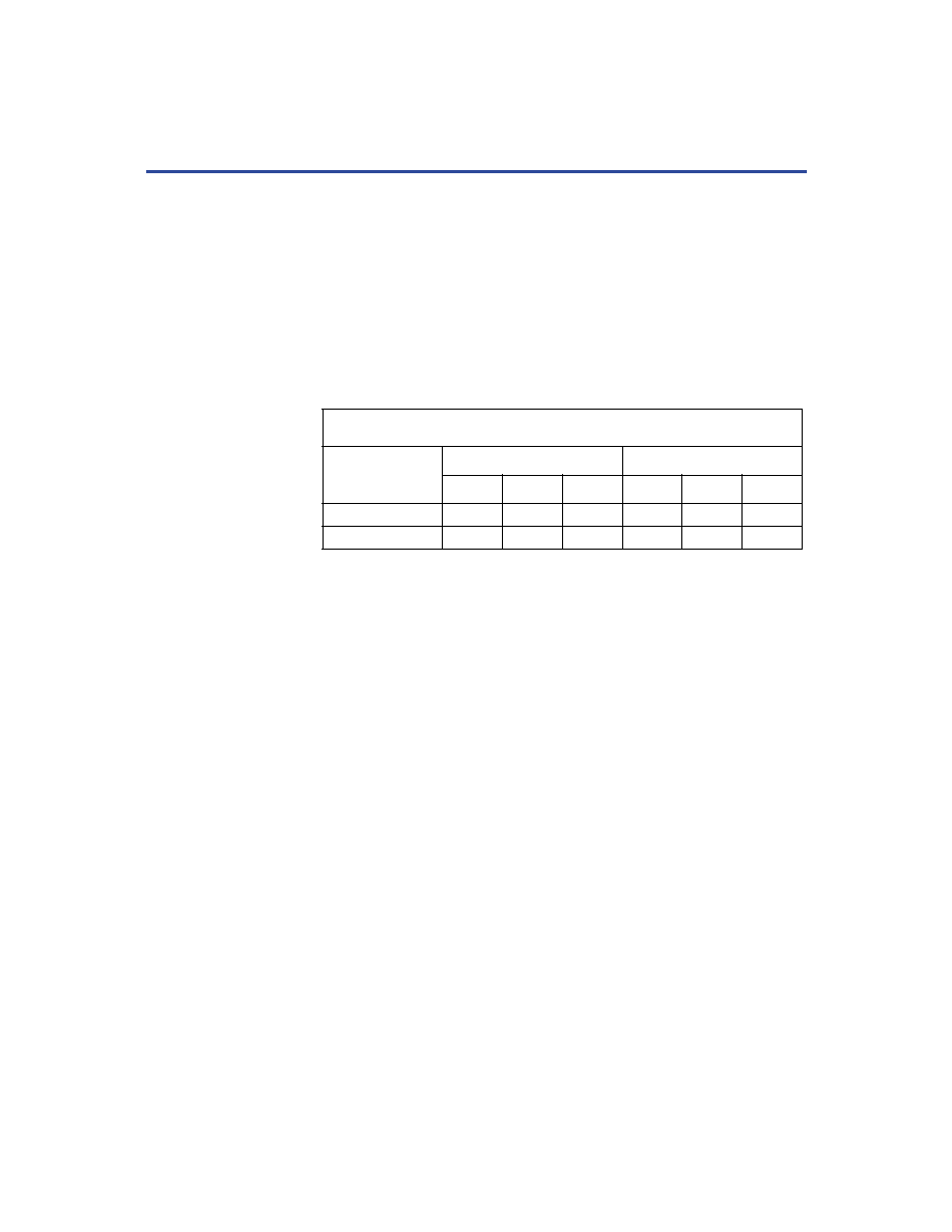
Table 13. ACEX 1K MultiVolt I/O Support
VCCIO (V)
Input Signal (V)
Output Signal (V)
2.5
3.3
5.0
2.5
3.3
5.0
2.5
v
v
3.3
vv
v (1)
v (2)
vv
相关PDF资料 |
PDF描述 |
|---|---|
| EP1K50FI484-1F | Field Programmable Gate Array (FPGA) |
| EP1K50FI484-1P | Field Programmable Gate Array (FPGA) |
| EP1K50FI484-1X | Field Programmable Gate Array (FPGA) |
| EP1K50FI484-2DX | Field Programmable Gate Array (FPGA) |
| EP1K50FI484-2F | Field Programmable Gate Array (FPGA) |
相关代理商/技术参数 |
参数描述 |
|---|---|
| EP1K50FC484-2N | 功能描述:FPGA - 现场可编程门阵列 FPGA - ACEX 1K 360 LABs 249 IOs RoHS:否 制造商:Altera Corporation 系列:Cyclone V E 栅极数量: 逻辑块数量:943 内嵌式块RAM - EBR:1956 kbit 输入/输出端数量:128 最大工作频率:800 MHz 工作电源电压:1.1 V 最大工作温度:+ 70 C 安装风格:SMD/SMT 封装 / 箱体:FBGA-256 |
| EP1K50FC484-2P | 制造商:未知厂家 制造商全称:未知厂家 功能描述:Field Programmable Gate Array (FPGA) |
| EP1K50FC484-2X | 制造商:未知厂家 制造商全称:未知厂家 功能描述:Field Programmable Gate Array (FPGA) |
| EP1K50FC484-3 | 功能描述:FPGA - 现场可编程门阵列 FPGA - ACEX 1K 360 LABs 249 IOs RoHS:否 制造商:Altera Corporation 系列:Cyclone V E 栅极数量: 逻辑块数量:943 内嵌式块RAM - EBR:1956 kbit 输入/输出端数量:128 最大工作频率:800 MHz 工作电源电压:1.1 V 最大工作温度:+ 70 C 安装风格:SMD/SMT 封装 / 箱体:FBGA-256 |
| EP1K50FC484-3F | 制造商:未知厂家 制造商全称:未知厂家 功能描述:Field Programmable Gate Array (FPGA) |
发布紧急采购,3分钟左右您将得到回复。