- 您现在的位置:买卖IC网 > PDF目录295885 > EP1SGX25FF1020C7ES (ALTERA CORP) FPGA, PBGA1020 PDF资料下载
参数资料
| 型号: | EP1SGX25FF1020C7ES |
| 厂商: | ALTERA CORP |
| 元件分类: | FPGA |
| 英文描述: | FPGA, PBGA1020 |
| 封装: | 33 X 33 MM, 1 MM PITCH, FBGA-1020 |
| 文件页数: | 62/279页 |
| 文件大小: | 3671K |
| 代理商: | EP1SGX25FF1020C7ES |
第1页第2页第3页第4页第5页第6页第7页第8页第9页第10页第11页第12页第13页第14页第15页第16页第17页第18页第19页第20页第21页第22页第23页第24页第25页第26页第27页第28页第29页第30页第31页第32页第33页第34页第35页第36页第37页第38页第39页第40页第41页第42页第43页第44页第45页第46页第47页第48页第49页第50页第51页第52页第53页第54页第55页第56页第57页第58页第59页第60页第61页当前第62页第63页第64页第65页第66页第67页第68页第69页第70页第71页第72页第73页第74页第75页第76页第77页第78页第79页第80页第81页第82页第83页第84页第85页第86页第87页第88页第89页第90页第91页第92页第93页第94页第95页第96页第97页第98页第99页第100页第101页第102页第103页第104页第105页第106页第107页第108页第109页第110页第111页第112页第113页第114页第115页第116页第117页第118页第119页第120页第121页第122页第123页第124页第125页第126页第127页第128页第129页第130页第131页第132页第133页第134页第135页第136页第137页第138页第139页第140页第141页第142页第143页第144页第145页第146页第147页第148页第149页第150页第151页第152页第153页第154页第155页第156页第157页第158页第159页第160页第161页第162页第163页第164页第165页第166页第167页第168页第169页第170页第171页第172页第173页第174页第175页第176页第177页第178页第179页第180页第181页第182页第183页第184页第185页第186页第187页第188页第189页第190页第191页第192页第193页第194页第195页第196页第197页第198页第199页第200页第201页第202页第203页第204页第205页第206页第207页第208页第209页第210页第211页第212页第213页第214页第215页第216页第217页第218页第219页第220页第221页第222页第223页第224页第225页第226页第227页第228页第229页第230页第231页第232页第233页第234页第235页第236页第237页第238页第239页第240页第241页第242页第243页第244页第245页第246页第247页第248页第249页第250页第251页第252页第253页第254页第255页第256页第257页第258页第259页第260页第261页第262页第263页第264页第265页第266页第267页第268页第269页第270页第271页第272页第273页第274页第275页第276页第277页第278页第279页
4–88
Altera Corporation
Stratix GX Device Handbook, Volume 1
February 2005
PLLs & Clock Networks
pair of output pins (four pins total) has dedicated
VCC and GND pins to
reduce the output clock’s overall jitter by providing improved isolation
from switching I/O pins.
For PLLs 5 and 6, each pin of a single-ended output pair can either be in
phase or 180° out of phase. The clock output pin pairs support the same
I/O standards as standard output pins (in the top and bottom banks) as
well as LVDS, LVPECL, 3.3-V PCML, HyperTransport technology,
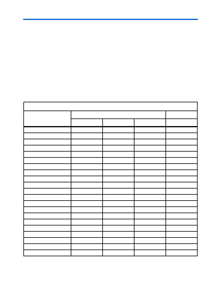
differential HSTL, and differential SSTL. Table 4–19 shows which I/O
standards the enhanced PLL clock pins support. When in single-ended or
differential mode, the two outputs operate off the same power supply.
Both outputs use the same standards in single-ended mode to maintain
performance. You can also use the external clock output pins as user
output pins if external enhanced PLL clocking is not needed.
Table 4–19. I/O Standards Supported for Enhanced PLL Pins (Part 1 of 2)
I/O Standard
Input
Output
INCLK
FBIN
PLLENABLE
EXTCLK
LVTTL
vvvv
LVCMOS
vvvv
2.5 V
vv
v
1.8 V
vv
v
1.5 V
vv
v
3.3-V PCI
vv
v
3.3-V PCI-X
vv
v
LVPECL
vv
v
3.3-V PCML
vv
v
LVDS
vv
v
HyperTransport technology
vv
v
Differential HSTL
vv
Differential SSTL
v
3.3-V GTL
vv
v
3.3-V GTL+
vv
v
1.5-V HSTL class I
vv
v
1.5-V HSTL class II
vv
v
SSTL-18 class I
vv
v
SSTL-18 class II
vv
v
SSTL-2 class I
vv
v
SSTL-2 class II
vv
v
相关PDF资料 |
PDF描述 |
|---|---|
| EP1SGX25FF1020I5ES | FPGA, PBGA1020 |
| EP1SGX25FF1020I5N | FPGA, PBGA1020 |
| EP1SGX25FF1020I6ES | FPGA, PBGA1020 |
| EP1SGX25FF1020I7ES | FPGA, PBGA1020 |
| EP1SGX25FF1020I7N | FPGA, PBGA1020 |
相关代理商/技术参数 |
参数描述 |
|---|---|
| EP1SGX25FF1020C7N | 功能描述:FPGA - 现场可编程门阵列 FPGA - Stratix I GX 2566 LABs 607 IOs RoHS:否 制造商:Altera Corporation 系列:Cyclone V E 栅极数量: 逻辑块数量:943 内嵌式块RAM - EBR:1956 kbit 输入/输出端数量:128 最大工作频率:800 MHz 工作电源电压:1.1 V 最大工作温度:+ 70 C 安装风格:SMD/SMT 封装 / 箱体:FBGA-256 |
| EP1SGX25FF1020I6 | 功能描述:FPGA - 现场可编程门阵列 FPGA - Stratix I GX 2566 LABs 607 IOs RoHS:否 制造商:Altera Corporation 系列:Cyclone V E 栅极数量: 逻辑块数量:943 内嵌式块RAM - EBR:1956 kbit 输入/输出端数量:128 最大工作频率:800 MHz 工作电源电压:1.1 V 最大工作温度:+ 70 C 安装风格:SMD/SMT 封装 / 箱体:FBGA-256 |
| EP1SGX25FF1020I6N | 功能描述:FPGA - 现场可编程门阵列 FPGA - Stratix I GX 2566 LABs 607 IOs RoHS:否 制造商:Altera Corporation 系列:Cyclone V E 栅极数量: 逻辑块数量:943 内嵌式块RAM - EBR:1956 kbit 输入/输出端数量:128 最大工作频率:800 MHz 工作电源电压:1.1 V 最大工作温度:+ 70 C 安装风格:SMD/SMT 封装 / 箱体:FBGA-256 |
| EP1SGX40 | 制造商:ALTERA 制造商全称:Altera Corporation 功能描述:1. Enhanced Configuration Devices (EPC4, EPC8, and EPC16) Data Sheet |
| EP1SGX40D | 制造商:ALTERA 制造商全称:Altera Corporation 功能描述:StratixGX FPGA Family |
发布紧急采购,3分钟左右您将得到回复。