- 您现在的位置:买卖IC网 > PDF目录299031 > EP20K100BC672-2 (ALTERA CORP) LOADABLE PLD, PBGA672 PDF资料下载
参数资料
| 型号: | EP20K100BC672-2 |
| 厂商: | ALTERA CORP |
| 元件分类: | PLD |
| 英文描述: | LOADABLE PLD, PBGA672 |
| 文件页数: | 32/68页 |
| 文件大小: | 975K |
| 代理商: | EP20K100BC672-2 |
第1页第2页第3页第4页第5页第6页第7页第8页第9页第10页第11页第12页第13页第14页第15页第16页第17页第18页第19页第20页第21页第22页第23页第24页第25页第26页第27页第28页第29页第30页第31页当前第32页第33页第34页第35页第36页第37页第38页第39页第40页第41页第42页第43页第44页第45页第46页第47页第48页第49页第50页第51页第52页第53页第54页第55页第56页第57页第58页第59页第60页第61页第62页第63页第64页第65页第66页第67页第68页
38
4317K–AVR–03/2013
AT90PWM2/3/2B/3B
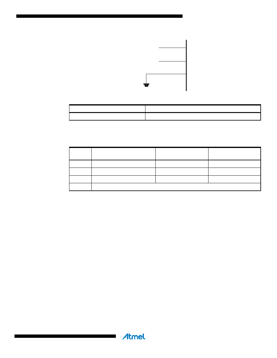
Figure 7-6.
External Clock Drive Configuration
When this clock source is selected, start-up times are determined by the SUT Fuses as shown in
When applying an external clock, it is required to avoid sudden changes in the applied clock fre-
quency to ensure stable operation of the MCU. A variation in frequency of more than 2% from
one clock cycle to the next can lead to unpredictable behavior. It is required to ensure that the
MCU is kept in Reset during such changes in the clock frequency.
Note that the System Clock Prescaler can be used to implement run-time changes of the internal
clock frequency while still ensuring stable operation. Refer to “System Clock Prescaler” on page
38 for details.
7.9
Clock Output Buffer
When the CKOUT Fuse is programmed, the system Clock will be output on CLKO. This mode is
suitable when chip clock is used to drive other circuits on the system. The clock will be output
also during reset and the normal operation of I/O pin will be overridden when the fuse is pro-
grammed. Any clock source, including internal RC Oscillator, can be selected when CLKO
serves as clock output. If the System Clock Prescaler is used, it is the divided system clock that
is output (CKOUT Fuse programmed).
7.10
System Clock Prescaler
The AT90PWM2/2B/3/3B system clock can be divided by setting the Clock Prescale Register –
CLKPR. This feature can be used to decrease power consumption when the requirement for
processing power is low. This can be used with all clock source options, and it will affect the
clock frequency of the CPU and all synchronous peripherals. clk
I/O, clkADC, clkCPU, and clkFLASH
are divided by a factor as shown in Table 7-12.
Table 7-10.
External Clock Frequency
CKSEL3..0
Frequency Range
0000
0 - 16 MHz
Table 7-11.
Start-up Times for the External Clock Selection
SUT1..0
Start-up Time from Power-
down and Power-save
Additional Delay from
Reset (VCC = 5.0V)
Recommended Usage
00
6 CK
14CK
BOD enabled
01
6 CK
14CK + 4.1 ms
Fast rising power
10
6 CK
14CK + 65 ms
Slowly rising power
11
Reserved
XTAL2
XTAL1
GND
NC
External
Clock
Signal
相关PDF资料 |
PDF描述 |
|---|---|
| EP20K100BC672-3 | LOADABLE PLD, PBGA672 |
| EP20K100BI672-1 | LOADABLE PLD, PBGA672 |
| EP20K100BI672-2 | LOADABLE PLD, PBGA672 |
| EP20K100BI672-3 | LOADABLE PLD, PBGA672 |
| EP20K100EFC400-1 | LOADABLE PLD, PBGA400 |
相关代理商/技术参数 |
参数描述 |
|---|---|
| EP20K100BI356-1 | 制造商:未知厂家 制造商全称:未知厂家 功能描述:Field Programmable Gate Array (FPGA) |
| EP20K100BI356-1ES | 制造商:未知厂家 制造商全称:未知厂家 功能描述:FPGA |
| EP20K100BI356-2 | 制造商:未知厂家 制造商全称:未知厂家 功能描述:Field Programmable Gate Array (FPGA) |
| EP20K100BI356-2ES | 制造商:未知厂家 制造商全称:未知厂家 功能描述:FPGA |
| EP20K100BI356-3 | 制造商:未知厂家 制造商全称:未知厂家 功能描述:Field Programmable Gate Array (FPGA) |
发布紧急采购,3分钟左右您将得到回复。