参数资料
| 型号: | EP2AGX260EF29I5N |
| 厂商: | Altera |
| 文件页数: | 83/90页 |
| 文件大小: | 0K |
| 描述: | IC ARRIA II GX FPGA 260K 780FBGA |
| 产品培训模块: | Three Reasons to Use FPGA's in Industrial Designs |
| 标准包装: | 4 |
| 系列: | Arria II GX |
| LAB/CLB数: | 10260 |
| 逻辑元件/单元数: | 244188 |
| RAM 位总计: | 12038144 |
| 输入/输出数: | 372 |
| 电源电压: | 0.87 V ~ 0.93 V |
| 安装类型: | 表面贴装 |
| 工作温度: | -40°C ~ 100°C |
| 封装/外壳: | 780-BBGA |
| 供应商设备封装: | 780-FBGA(29x29) |
第1页第2页第3页第4页第5页第6页第7页第8页第9页第10页第11页第12页第13页第14页第15页第16页第17页第18页第19页第20页第21页第22页第23页第24页第25页第26页第27页第28页第29页第30页第31页第32页第33页第34页第35页第36页第37页第38页第39页第40页第41页第42页第43页第44页第45页第46页第47页第48页第49页第50页第51页第52页第53页第54页第55页第56页第57页第58页第59页第60页第61页第62页第63页第64页第65页第66页第67页第68页第69页第70页第71页第72页第73页第74页第75页第76页第77页第78页第79页第80页第81页第82页当前第83页第84页第85页第86页第87页第88页第89页第90页
1–76
Chapter 1: Device Datasheet for Arria II Devices
Glossary
December 2013
Altera Corporation
S
SW (sampling
window)
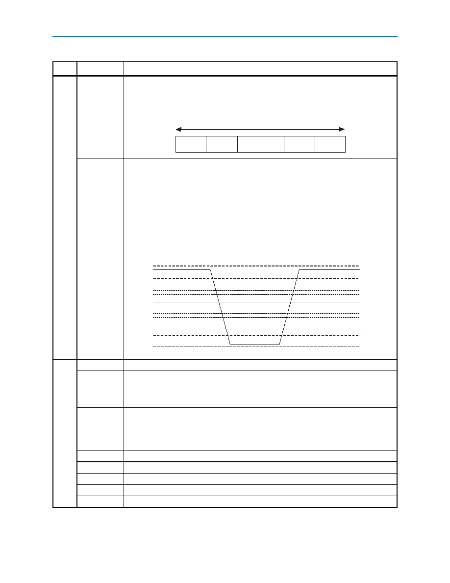
The period of time during which the data must be valid in order to capture it correctly. The setup
and hold times determine the ideal strobe position within the sampling window:
Timing Diagram
Single-ended
Voltage
Referenced I/O
Standard
The JEDEC standard for SSTL and HSTL I/O standards define both the AC and DC input signal
values. The AC values indicate the voltage levels at which the receiver must meet its timing
specifications. The DC values indicate the voltage levels at which the final logic state of the
receiver is unambiguously defined. After the receiver input has crossed the AC value, the receiver
changes to the new logic state.
The new logic state is then maintained as long as the input stays beyond the AC threshold. This
approach is intended to provide predictable receiver timing in the presence of input waveform
ringing:
Single-Ended Voltage Referenced I/O Standard
T
tC
High-speed receiver and transmitter input and output clock period.
TCCS
(channel-to-
channel-
skew)
The timing difference between the fastest and slowest output edges, including tCO variation and
clock skew, across channels driven by the same PLL. The clock is included in the TCCS
measurement (refer to the Timing Diagram figure under S in this table).
tDUTY
High-speed I/O block: Duty cycle on the high-speed transmitter output clock.
Timing Unit Interval (TUI)
The timing budget allowed for skew, propagation delays, and data sampling window.
(TUI = 1/(Receiver Input Clock Frequency Multiplication Factor) = tC/w)
tFALL
Signal high-to-low transition time (80-20%)
tINCCJ
Cycle-to-cycle jitter tolerance on the PLL clock input.
tOUTPJ_IO
Period jitter on the general purpose I/O driven by a PLL.
tOUTPJ_DC
Period jitter on the dedicated clock output driven by a PLL.
tRISE
Signal low-to-high transition time (20-80%).
Table 1–68. Glossary (Part 3 of 4)
Letter
Subject
Definitions
Bit Time
0.5 x TCCS
RSKM
Sampling Window
(SW)
RSKM
0.5 x TCCS
VIH(AC)
VIH(DC)
VREF
VIL(DC)
VIL(AC)
VOH
VOL
VCCIO
VSS
相关PDF资料 |
PDF描述 |
|---|---|
| AGM36DTAD-S189 | CONN EDGECARD 72POS R/A .156 SLD |
| EP2AGX190FF35I3N | IC ARRIA II GX 190K 1152FBGA |
| RSC60DRTI-S734 | CONN EDGECARD 120PS DIP .100 SLD |
| EP1S40F1508C5N | IC STRATIX FPGA 40K LE 1508-FBGA |
| RMC60DRTI-S734 | CONN EDGECARD 120PS DIP .100 SLD |
相关代理商/技术参数 |
参数描述 |
|---|---|
| EP2AGX260FF35C4 | 功能描述:FPGA - 现场可编程门阵列 FPGA - Arria II GX 10260 LABs 612 IO RoHS:否 制造商:Altera Corporation 系列:Cyclone V E 栅极数量: 逻辑块数量:943 内嵌式块RAM - EBR:1956 kbit 输入/输出端数量:128 最大工作频率:800 MHz 工作电源电压:1.1 V 最大工作温度:+ 70 C 安装风格:SMD/SMT 封装 / 箱体:FBGA-256 |
| EP2AGX260FF35C4N | 功能描述:FPGA - 现场可编程门阵列 FPGA - Arria II GX 10260 LABs 612 IO RoHS:否 制造商:Altera Corporation 系列:Cyclone V E 栅极数量: 逻辑块数量:943 内嵌式块RAM - EBR:1956 kbit 输入/输出端数量:128 最大工作频率:800 MHz 工作电源电压:1.1 V 最大工作温度:+ 70 C 安装风格:SMD/SMT 封装 / 箱体:FBGA-256 |
| EP2AGX260FF35C5 | 功能描述:FPGA - 现场可编程门阵列 FPGA - Arria II GX 10260 LABs 612 IO RoHS:否 制造商:Altera Corporation 系列:Cyclone V E 栅极数量: 逻辑块数量:943 内嵌式块RAM - EBR:1956 kbit 输入/输出端数量:128 最大工作频率:800 MHz 工作电源电压:1.1 V 最大工作温度:+ 70 C 安装风格:SMD/SMT 封装 / 箱体:FBGA-256 |
| EP2AGX260FF35C5N | 功能描述:FPGA - 现场可编程门阵列 FPGA - Arria II GX 10260 LABs 612 IO RoHS:否 制造商:Altera Corporation 系列:Cyclone V E 栅极数量: 逻辑块数量:943 内嵌式块RAM - EBR:1956 kbit 输入/输出端数量:128 最大工作频率:800 MHz 工作电源电压:1.1 V 最大工作温度:+ 70 C 安装风格:SMD/SMT 封装 / 箱体:FBGA-256 |
| EP2AGX260FF35C6 | 功能描述:FPGA - 现场可编程门阵列 FPGA - Arria II GX 10260 LABs 612 IO RoHS:否 制造商:Altera Corporation 系列:Cyclone V E 栅极数量: 逻辑块数量:943 内嵌式块RAM - EBR:1956 kbit 输入/输出端数量:128 最大工作频率:800 MHz 工作电源电压:1.1 V 最大工作温度:+ 70 C 安装风格:SMD/SMT 封装 / 箱体:FBGA-256 |
发布紧急采购,3分钟左右您将得到回复。