- 您现在的位置:买卖IC网 > PDF目录19319 > EP2AGX260FF35C4N (Altera)IC ARRIAII GX FPGA 260K 1152FBGA PDF资料下载
参数资料
| 型号: | EP2AGX260FF35C4N |
| 厂商: | Altera |
| 文件页数: | 76/90页 |
| 文件大小: | 0K |
| 描述: | IC ARRIAII GX FPGA 260K 1152FBGA |
| 产品培训模块: | Three Reasons to Use FPGA's in Industrial Designs |
| 标准包装: | 3 |
| 系列: | Arria II GX |
| LAB/CLB数: | 10260 |
| 逻辑元件/单元数: | 244188 |
| RAM 位总计: | 12038144 |
| 输入/输出数: | 612 |
| 电源电压: | 0.87 V ~ 0.93 V |
| 安装类型: | 表面贴装 |
| 工作温度: | 0°C ~ 85°C |
| 封装/外壳: | 1152-BBGA |
| 供应商设备封装: | 1152-FBGA(27x27) |
| 配用: | 568-5095-ND - BOARD DEMO FOR ADC1413D125 |
| 其它名称: | 544-2698 |
第1页第2页第3页第4页第5页第6页第7页第8页第9页第10页第11页第12页第13页第14页第15页第16页第17页第18页第19页第20页第21页第22页第23页第24页第25页第26页第27页第28页第29页第30页第31页第32页第33页第34页第35页第36页第37页第38页第39页第40页第41页第42页第43页第44页第45页第46页第47页第48页第49页第50页第51页第52页第53页第54页第55页第56页第57页第58页第59页第60页第61页第62页第63页第64页第65页第66页第67页第68页第69页第70页第71页第72页第73页第74页第75页当前第76页第77页第78页第79页第80页第81页第82页第83页第84页第85页第86页第87页第88页第89页第90页
1–70
Chapter 1: Device Datasheet for Arria II Devices
Switching Characteristics
December 2013
Altera Corporation
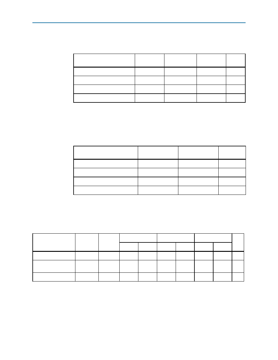
Table 1–60 lists the DQS phase shift error for Arria II GX devices.
Table 1–61 lists the DQS phase shift error for Arria II GZ devices.
Table 1–62 lists the memory output clock jitter specifications for Arria II GX devices.
Table 1–60. DQS Phase Shift Error Specification for DLL-Delayed Clock (tDQS_PSERR) for Arria II GX
Devices (Note 1)
Number of DQS Delay Buffer
C4
I3, C5, I5
C6
Unit
1
263036
ps
2
526072
ps
3
78
90
108
ps
4
104
120
144
ps
Note to Table 1–60:
(1) This error specification is the absolute maximum and minimum error. For example, skew on three DQS delay
buffers in a C4 speed grade is ± 78 ps or ± 39 ps.
Table 1–61. DQS Phase Shift Error Specification for DLL-Delayed Clock (tDQS_PSERR) for Arria II GZ
Devices (Note 1)
Number of DQS Delay Buffer
–3
–4
Unit
128
30
ps
256
60
ps
384
90
ps
4
112
120
ps
Note to Table 1–61:
(1) This error specification is the absolute maximum and minimum error. For example, skew on three DQS delay
buffers in a 3 speed grade is ± 84 ps or ± 42 ps.
Parameter
Clock
Network
Symbol
–4
–5
–6
Unit
Min
Max
Min
Max
Min
Max
Clock period jitter
Global
t
JIT(per)
-100
100
-125
125
-125
125
ps
Cycle-to-cycle period
jitter
Global
t
JIT(cc)
-200
200
-250
250
-250
250
ps
Duty cycle jitter
Global
t
JIT(duty)
-100
100
-125
125
-125
125
ps
Notes to Table 1–62:
(1) The memory output clock jitter measurements are for 200 consecutive clock cycles, as specified in the JEDEC DDR2/DDR3 SDRAM standard.
(2) The clock jitter specification applies to memory output clock pins generated using DDIO circuits clocked by a PLL output routed on a global
clock network.
(3) The memory output clock jitter stated in Table 1–62 is applicable when an input jitter of 30 ps is applied.
相关PDF资料 |
PDF描述 |
|---|---|
| VE-262-CY-S | CONVERTER MOD DC/DC 15V 50W |
| RAC05-05DA-E-ST | CONV AC/DC 90-264VAC +/-5V 500MA |
| VI-BTF-CV-F4 | CONVERTER MOD DC/DC 72V 150W |
| VE-21K-CW-F4 | CONVERTER MOD DC/DC 40V 100W |
| AMC30DREF-S734 | CONN EDGECARD 60POS .100 EYELET |
相关代理商/技术参数 |
参数描述 |
|---|---|
| EP2AGX260FF35C5 | 功能描述:FPGA - 现场可编程门阵列 FPGA - Arria II GX 10260 LABs 612 IO RoHS:否 制造商:Altera Corporation 系列:Cyclone V E 栅极数量: 逻辑块数量:943 内嵌式块RAM - EBR:1956 kbit 输入/输出端数量:128 最大工作频率:800 MHz 工作电源电压:1.1 V 最大工作温度:+ 70 C 安装风格:SMD/SMT 封装 / 箱体:FBGA-256 |
| EP2AGX260FF35C5N | 功能描述:FPGA - 现场可编程门阵列 FPGA - Arria II GX 10260 LABs 612 IO RoHS:否 制造商:Altera Corporation 系列:Cyclone V E 栅极数量: 逻辑块数量:943 内嵌式块RAM - EBR:1956 kbit 输入/输出端数量:128 最大工作频率:800 MHz 工作电源电压:1.1 V 最大工作温度:+ 70 C 安装风格:SMD/SMT 封装 / 箱体:FBGA-256 |
| EP2AGX260FF35C6 | 功能描述:FPGA - 现场可编程门阵列 FPGA - Arria II GX 10260 LABs 612 IO RoHS:否 制造商:Altera Corporation 系列:Cyclone V E 栅极数量: 逻辑块数量:943 内嵌式块RAM - EBR:1956 kbit 输入/输出端数量:128 最大工作频率:800 MHz 工作电源电压:1.1 V 最大工作温度:+ 70 C 安装风格:SMD/SMT 封装 / 箱体:FBGA-256 |
| EP2AGX260FF35C6N | 功能描述:FPGA - 现场可编程门阵列 FPGA - Arria II GX 10260 LABs 612 IO RoHS:否 制造商:Altera Corporation 系列:Cyclone V E 栅极数量: 逻辑块数量:943 内嵌式块RAM - EBR:1956 kbit 输入/输出端数量:128 最大工作频率:800 MHz 工作电源电压:1.1 V 最大工作温度:+ 70 C 安装风格:SMD/SMT 封装 / 箱体:FBGA-256 |
| EP2AGX260FF35C6NES | 制造商:Altera Corporation 功能描述:IC FPGA 612 I/O 1152FBGA 制造商:Altera Corporation 功能描述:IC ARRIA II GX FPGA 1152FBGA |
发布紧急采购,3分钟左右您将得到回复。