参数资料
| 型号: | EP2AGX95EF35C5N |
| 厂商: | Altera |
| 文件页数: | 61/90页 |
| 文件大小: | 0K |
| 描述: | IC ARRIA II GX FPGA 95K 1152FBGA |
| 产品培训模块: | Three Reasons to Use FPGA's in Industrial Designs |
| 标准包装: | 3 |
| 系列: | Arria II GX |
| LAB/CLB数: | 3747 |
| 逻辑元件/单元数: | 89178 |
| RAM 位总计: | 6839296 |
| 输入/输出数: | 452 |
| 电源电压: | 0.87 V ~ 0.93 V |
| 安装类型: | 表面贴装 |
| 工作温度: | 0°C ~ 85°C |
| 封装/外壳: | 1152-BBGA |
| 供应商设备封装: | 1152-FBGA(27x27) |
第1页第2页第3页第4页第5页第6页第7页第8页第9页第10页第11页第12页第13页第14页第15页第16页第17页第18页第19页第20页第21页第22页第23页第24页第25页第26页第27页第28页第29页第30页第31页第32页第33页第34页第35页第36页第37页第38页第39页第40页第41页第42页第43页第44页第45页第46页第47页第48页第49页第50页第51页第52页第53页第54页第55页第56页第57页第58页第59页第60页当前第61页第62页第63页第64页第65页第66页第67页第68页第69页第70页第71页第72页第73页第74页第75页第76页第77页第78页第79页第80页第81页第82页第83页第84页第85页第86页第87页第88页第89页第90页
1–56
Chapter 1: Device Datasheet for Arria II Devices
Switching Characteristics
December 2013
Altera Corporation
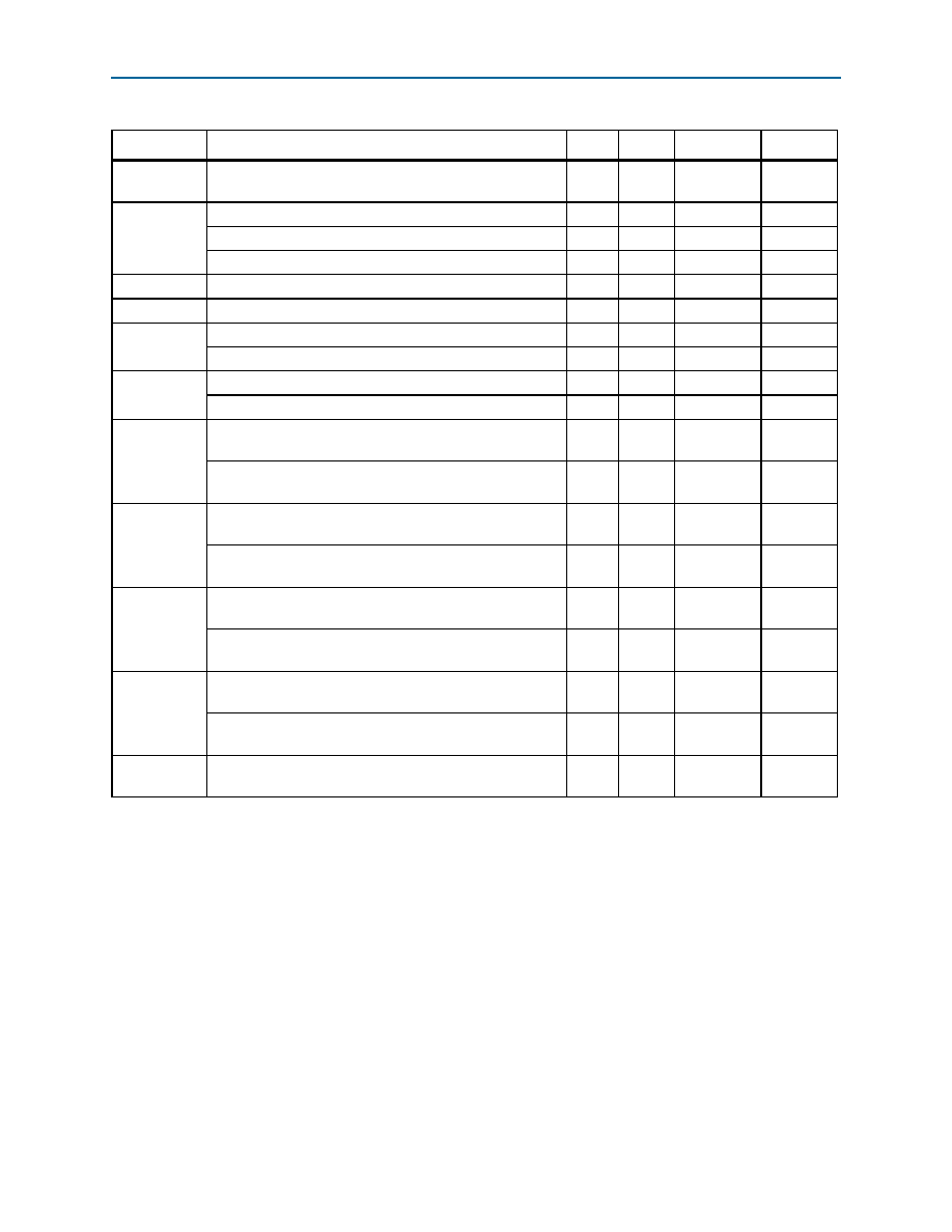
tDLOCK
Time required to lock dynamically (after switchover or
reconfiguring any non-post-scale counters/delays)
——
1
ms
fCLBW
PLL closed-loop low bandwidth
—
0.3
—
MHz
PLL closed-loop medium bandwidth
—
1.5
—
MHz
PLL closed-loop high bandwidth (7)
—4
—
MHz
tPLL_PSERR
Accuracy of PLL phase shift
—
±50
ps
tARESET
Minimum pulse width on the areset signal
10
—
ns
Input clock cycle to cycle jitter (FREF ≥ 100 MHz)
—
0.15
UI (p-p)
Input clock cycle to cycle jitter (FREF < 100 MHz)
—
±750
ps (p-p)
tOUTPJ_DC (5)
Period Jitter for dedicated clock output (FOUT ≥ 100 MHz)
—
175
ps (p-p)
Period Jitter for dedicated clock output (FOUT < 100 MHz)
—
17.5
mUI (p-p)
tOUTCCJ_DC (5)
Cycle to Cycle Jitter for dedicated clock output
(FOUT ≥ 100 MHz)
—
175
ps (p-p)
Cycle to Cycle Jitter for dedicated clock output
(FOUT < 100 MHz)
—
17.5
mUI (p-p)
tOUTPJ_IO (5),
Period Jitter for clock output on regular I/O
(FOUT ≥ 100 MHz)
—
600
ps (p-p)
Period Jitter for clock output on regular I/O
(FOUT < 100 MHz)
—
60
mUI (p-p)
tOUTCCJ_IO (5),
Cycle to Cycle Jitter for clock output on regular I/O
(FOUT ≥ 100 MHz)
—
600
ps (p-p)
Cycle to Cycle Jitter for clock output on regular I/O
(FOUT < 100 MHz)
—
60
mUI (p-p)
tCASC_OUTPJ_DC
Period Jitter for dedicated clock output in cascaded PLLs
(FOUT ≥100MHz)
—
250
ps (p-p)
Period Jitter for dedicated clock output in cascaded PLLs
(FOUT < 100MHz)
—
25
mUI (p-p)
fDRIFT
Frequency drift after PFDENA is disabled for duration of
100 us
—
±10
%
Notes to Table 1–45:
(1) This specification is limited in the Quartus II software by the I/O maximum frequency. The maximum I/O frequency is different for each I/O
standard.
(2) This specification is limited by the lower of the two: I/O FMAX or FOUT of the PLL.
(3) A high input jitter directly affects the PLL output jitter. To have low PLL output clock jitter, you must provide a clean clock source that is less
than 120 ps.
(4) FREF is fIN/N when N = 1.
(5) Peak-to-peak jitter with a probability level of 10–12 (14 sigma, 99.99999999974404% confidence level). The output jitter specification applies
to the intrinsic jitter of the PLL, when an input jitter of 30 ps is applied. The external memory interface clock output jitter specifications use a
different measurement method and are available in Table 1–64 on page 1–71.
(6) The cascaded PLL specification is only applicable with the following condition:
a. Upstream PLL: 0.59 Mhz
Upstream PLL BW < 1 MHz
b. Downstream PLL: Downstream PLL BW > 2 MHz
(7) High bandwidth PLL settings are not supported in external feedback mode.
(8) External memory interface clock output jitter specifications use a different measurement method, which is available in Table 1–63 on
Table 1–45. PLL Specifications for Arria II GZ Devices (Part 2 of 2)
Symbol
Parameter
Min
Typ
Max
Unit
相关PDF资料 |
PDF描述 |
|---|---|
| 24LC00T/SN | IC EEPROM 128BIT 400KHZ 8SOIC |
| EP2SGX60DF780C5 | IC STRATIX II GX 60K 780-FBGA |
| 24LC00T-I/SN | IC EEPROM 128BIT 400KHZ 8SOIC |
| AMM24DTBD-S189 | CONN EDGECARD 48POS R/A .156 SLD |
| A1460A-PG207C | IC FPGA 6K GATES 207-CPGA |
相关代理商/技术参数 |
参数描述 |
|---|---|
| EP2AGX95EF35C5NES | 制造商:Altera Corporation 功能描述:IC ARRIA II GX FPGA 1152FBGA |
| EP2AGX95EF35C6 | 功能描述:FPGA - 现场可编程门阵列 FPGA - Arria II GX 3747 LABs 452 IOs RoHS:否 制造商:Altera Corporation 系列:Cyclone V E 栅极数量: 逻辑块数量:943 内嵌式块RAM - EBR:1956 kbit 输入/输出端数量:128 最大工作频率:800 MHz 工作电源电压:1.1 V 最大工作温度:+ 70 C 安装风格:SMD/SMT 封装 / 箱体:FBGA-256 |
| EP2AGX95EF35C6ES | 制造商:Altera Corporation 功能描述:FPGA Arria |
| EP2AGX95EF35C6N | 功能描述:FPGA - 现场可编程门阵列 FPGA - Arria II GX 3747 LABs 452 IOs RoHS:否 制造商:Altera Corporation 系列:Cyclone V E 栅极数量: 逻辑块数量:943 内嵌式块RAM - EBR:1956 kbit 输入/输出端数量:128 最大工作频率:800 MHz 工作电源电压:1.1 V 最大工作温度:+ 70 C 安装风格:SMD/SMT 封装 / 箱体:FBGA-256 |
| EP2AGX95EF35C6NES | 制造商:Altera Corporation 功能描述:FPGA Arria |
发布紧急采购,3分钟左右您将得到回复。