参数资料
| 型号: | EP4CE55F29C9LN |
| 厂商: | Altera |
| 文件页数: | 25/42页 |
| 文件大小: | 0K |
| 描述: | IC CYCLONE IV FPGA 55K 780FBGA |
| 产品培训模块: | Three Reasons to Use FPGA's in Industrial Designs Cyclone IV FPGA Family Overview |
| 特色产品: | Cyclone? IV FPGAs |
| 标准包装: | 36 |
| 系列: | CYCLONE® IV E |
| LAB/CLB数: | 3491 |
| 逻辑元件/单元数: | 55856 |
| RAM 位总计: | 2396160 |
| 输入/输出数: | 374 |
| 电源电压: | 0.97 V ~ 1.03 V |
| 安装类型: | 表面贴装 |
| 工作温度: | 0°C ~ 85°C |
| 封装/外壳: | 780-BBGA |
| 供应商设备封装: | 780-FBGA(29x29) |
第1页第2页第3页第4页第5页第6页第7页第8页第9页第10页第11页第12页第13页第14页第15页第16页第17页第18页第19页第20页第21页第22页第23页第24页当前第25页第26页第27页第28页第29页第30页第31页第32页第33页第34页第35页第36页第37页第38页第39页第40页第41页第42页
Chapter 1: Cyclone IV Device Datasheet
1–31
Switching Characteristics
December 2013
Altera Corporation
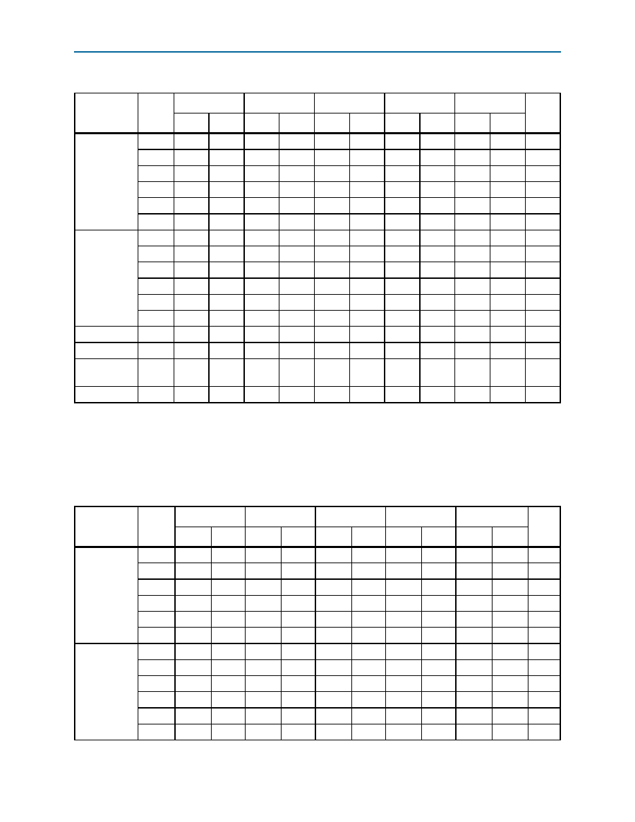
Table 1–34. True LVDS Transmitter Timing Specifications for Cyclone IV Devices (1), (3)
Symbol
Modes
C6
C7, I7
C8, A7
C8L, I8L
C9L
Unit
Min
Max
Min
Max
Min
Max
Min
Max
Min
Max
fHSCLK (input
clock
frequency)
×10
5
420
5
370
5
320
5
320
5
250
MHz
×8
5
420
5
370
5
320
5
320
5
250
MHz
×7
5
420
5
370
5
320
5
320
5
250
MHz
×4
5
420
5
370
5
320
5
320
5
250
MHz
×2
5
420
5
370
5
320
5
320
5
250
MHz
×1
5
420
5
402.5
5
402.5
5
362
5
265
MHz
HSIODR
×10
100
840
100
740
100
640
100
640
100
500
Mbps
×8
80
840
80
740
80
640
80
640
80
500
Mbps
×7
70
840
70
740
70
640
70
640
70
500
Mbps
×4
40
840
40
740
40
640
40
640
40
500
Mbps
×2
20
840
20
740
20
640
20
640
20
500
Mbps
×1
10
420
10
402.5
10
402.5
10
362
10
265
Mbps
tDUTY
—
4555
455545
55455545
55
%
TCCS
—
200
—
200
—
200
—
200
—
200
ps
Output jitter
(peak to peak)
—
500
—
500
—
550
—
600
—
700
ps
tLOCK (2)
—
—1—1
—1
ms
Notes to Table 1–34:
(1) Cyclone IV E—true LVDS transmitter is only supported at the output pin of Row I/O Banks 1, 2, 5, and 6.
Cyclone IV GX—true LVDS transmitter is only supported at the output pin of Row I/O Banks 5 and 6.
(2) tLOCK is the time required for the PLL to lock from the end-of-device configuration.
(3) Cyclone IV E 1.0 V core voltage devices only support C8L, C9L, and I8L speed grades. Cyclone IV E 1.2 V core voltage devices only support
C6, C7, C8, I7, and A7 speed grades. Cyclone IV GX devices only support C6, C7, C8, and I7 speed grades.
Table 1–35. Emulated LVDS Transmitter Timing Specifications for Cyclone IV Devices (1), (3) (Part 1 of 2)
Symbol
Modes
C6
C7, I7
C8, A7
C8L, I8L
C9L
Unit
Min
Max
Min
Max
Min
Max
Min
Max
Min
Max
fHSCLK (input
clock
frequency)
×10
5
320
5
320
5
275
5
275
5
250
MHz
×8
5
320
5
320
5
275
5
275
5
250
MHz
×7
5
320
5
320
5
275
5
275
5
250
MHz
×4
5
320
5
320
5
275
5
275
5
250
MHz
×2
5
320
5
320
5
275
5
275
5
250
MHz
×1
5
402.5
5
402.5
5
402.5
5
362
5
265
MHz
HSIODR
×10
100
640
100
640
100
550
100
550
100
500
Mbps
×8
80
640
80
640
80
550
80
550
80
500
Mbps
×7
70
640
70
640
70
550
70
550
70
500
Mbps
×4
40
640
40
640
40
550
40
550
40
500
Mbps
×2
20
640
20
640
20
550
20
550
20
500
Mbps
×1
10
402.5
10
402.5
10
402.5
10
362
10
265
Mbps
相关PDF资料 |
PDF描述 |
|---|---|
| EP4CE55F29C8N | IC CYCLONE IV FPGA 55K 780FBGA |
| A1010B-2PLG68I | IC FPGA 1200 GATES 68-PLCC IND |
| 955-009-020R121 | BACKSHELL 9POS Q-LOCK MET PLAS |
| 970-037-030R121 | BACKSHELL DB37 DIE CAST NICKEL |
| CAV24C08WE-GT3 | EEPROM I2C SER 8KB I2C 8SOIC |
相关代理商/技术参数 |
参数描述 |
|---|---|
| EP4CE55F29I7 | 功能描述:FPGA - 现场可编程门阵列 FPGA - Cyclone IV E 3491 LABs 374 IOs RoHS:否 制造商:Altera Corporation 系列:Cyclone V E 栅极数量: 逻辑块数量:943 内嵌式块RAM - EBR:1956 kbit 输入/输出端数量:128 最大工作频率:800 MHz 工作电源电压:1.1 V 最大工作温度:+ 70 C 安装风格:SMD/SMT 封装 / 箱体:FBGA-256 |
| EP4CE55F29I7N | 功能描述:FPGA - 现场可编程门阵列 FPGA - Cyclone IV E 3491 LABs 374 IOs RoHS:否 制造商:Altera Corporation 系列:Cyclone V E 栅极数量: 逻辑块数量:943 内嵌式块RAM - EBR:1956 kbit 输入/输出端数量:128 最大工作频率:800 MHz 工作电源电压:1.1 V 最大工作温度:+ 70 C 安装风格:SMD/SMT 封装 / 箱体:FBGA-256 |
| EP4CE55F29I8L | 功能描述:FPGA - 现场可编程门阵列 FPGA - Cyclone IV E 3491 LABs 374 IOs RoHS:否 制造商:Altera Corporation 系列:Cyclone V E 栅极数量: 逻辑块数量:943 内嵌式块RAM - EBR:1956 kbit 输入/输出端数量:128 最大工作频率:800 MHz 工作电源电压:1.1 V 最大工作温度:+ 70 C 安装风格:SMD/SMT 封装 / 箱体:FBGA-256 |
| EP4CE55F29I8LN | 功能描述:FPGA - 现场可编程门阵列 FPGA - Cyclone IV E 3491 LABs 374 IOs RoHS:否 制造商:Altera Corporation 系列:Cyclone V E 栅极数量: 逻辑块数量:943 内嵌式块RAM - EBR:1956 kbit 输入/输出端数量:128 最大工作频率:800 MHz 工作电源电压:1.1 V 最大工作温度:+ 70 C 安装风格:SMD/SMT 封装 / 箱体:FBGA-256 |
| EP4CE55U19I7N | 功能描述:FPGA - 现场可编程门阵列 FPGA - Cyclone IV E 3491 LABs 324 IOs RoHS:否 制造商:Altera Corporation 系列:Cyclone V E 栅极数量: 逻辑块数量:943 内嵌式块RAM - EBR:1956 kbit 输入/输出端数量:128 最大工作频率:800 MHz 工作电源电压:1.1 V 最大工作温度:+ 70 C 安装风格:SMD/SMT 封装 / 箱体:FBGA-256 |
发布紧急采购,3分钟左右您将得到回复。