参数资料
| 型号: | EP4CGX150DF31C7N |
| 厂商: | Altera |
| 文件页数: | 33/42页 |
| 文件大小: | 0K |
| 描述: | IC CYCLONE IV FPGA 150K 896FBGA |
| 产品培训模块: | Designing an IP Surveillance Camera Three Reasons to Use FPGA's in Industrial Designs Cyclone IV FPGA Family Overview |
| 特色产品: | Cyclone? IV FPGAs |
| 标准包装: | 27 |
| 系列: | CYCLONE® IV GX |
| LAB/CLB数: | 9360 |
| 逻辑元件/单元数: | 149760 |
| RAM 位总计: | 6635520 |
| 输入/输出数: | 475 |
| 电源电压: | 1.16 V ~ 1.24 V |
| 安装类型: | 表面贴装 |
| 工作温度: | 0°C ~ 85°C |
| 封装/外壳: | 896-BBGA |
| 供应商设备封装: | 896-FBGA(31x31) |
| 其它名称: | 544-2670 |
第1页第2页第3页第4页第5页第6页第7页第8页第9页第10页第11页第12页第13页第14页第15页第16页第17页第18页第19页第20页第21页第22页第23页第24页第25页第26页第27页第28页第29页第30页第31页第32页当前第33页第34页第35页第36页第37页第38页第39页第40页第41页第42页
Chapter 1: Cyclone IV Device Datasheet
1–39
Glossary
December 2013
Altera Corporation
R
RL
Receiver differential input discrete resistor (external to Cyclone IV devices).
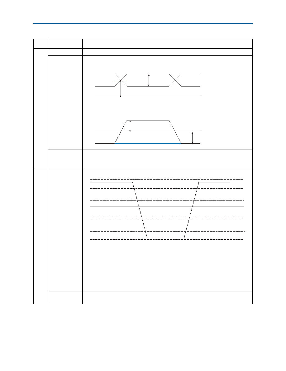
Receiver Input
Waveform
Receiver input waveform for LVDS and LVPECL differential standards:
Receiver input
skew margin
(RSKM)
High-speed I/O block: The total margin left after accounting for the sampling window and TCCS.
RSKM = (TUI – SW – TCCS) / 2.
S
Single-ended
voltage-
referenced I/O
Standard
The JEDEC standard for SSTl and HSTL I/O standards defines both the AC and DC input signal
values. The AC values indicate the voltage levels at which the receiver must meet its timing
specifications. The DC values indicate the voltage levels at which the final logic state of the
receiver is unambiguously defined. After the receiver input crosses the AC value, the receiver
changes to the new logic state. The new logic state is then maintained as long as the input stays
beyond the DC threshold. This approach is intended to provide predictable receiver timing in the
presence of input waveform ringing.
SW (Sampling
Window)
High-speed I/O block: The period of time during which the data must be valid to capture it
correctly. The setup and hold times determine the ideal strobe position in the sampling window.
Table 1–46. Glossary (Part 3 of 5)
Letter
Term
Definitions
Single-Ended Waveform
Differential Waveform (Mathematical Function of Positive & Negative Channel)
Positive Channel (p) = V
IH
Negative Channel (n) = V
IL
Ground
V
ID
V
ID
0 V
V
CM
p
- n
V
ID
VIH(AC)
VIH(DC)
VREF
VIL(DC)
VIL(AC)
VOH
VOL
VCCIO
VSS
相关PDF资料 |
PDF描述 |
|---|---|
| AX1000-2FG896I | IC FPGA AXCELERATOR 1M 896-FBGA |
| RSA50DRMZ-S273 | CONN EDGECARD 100POS .125 SQ WW |
| RMA50DRMZ-S273 | CONN EDGECARD 100POS .125 SQ WW |
| A42MX36-3BG272 | IC FPGA MX SGL CHIP 54K 272-PBGA |
| FMC19DRYN-S93 | CONN EDGECARD 38POS .100 DIP SLD |
相关代理商/技术参数 |
参数描述 |
|---|---|
| EP4CGX150DF31C8 | 功能描述:FPGA - 现场可编程门阵列 FPGA - Cyclone IV GX 9360 LABs 475 IOs RoHS:否 制造商:Altera Corporation 系列:Cyclone V E 栅极数量: 逻辑块数量:943 内嵌式块RAM - EBR:1956 kbit 输入/输出端数量:128 最大工作频率:800 MHz 工作电源电压:1.1 V 最大工作温度:+ 70 C 安装风格:SMD/SMT 封装 / 箱体:FBGA-256 |
| EP4CGX150DF31C8N | 功能描述:FPGA - 现场可编程门阵列 FPGA - Cyclone IV GX 9360 LABs 475 IOs RoHS:否 制造商:Altera Corporation 系列:Cyclone V E 栅极数量: 逻辑块数量:943 内嵌式块RAM - EBR:1956 kbit 输入/输出端数量:128 最大工作频率:800 MHz 工作电源电压:1.1 V 最大工作温度:+ 70 C 安装风格:SMD/SMT 封装 / 箱体:FBGA-256 |
| EP4CGX150DF31I7 | 功能描述:FPGA - 现场可编程门阵列 FPGA - Cyclone IV GX 9360 LABs 475 IOs RoHS:否 制造商:Altera Corporation 系列:Cyclone V E 栅极数量: 逻辑块数量:943 内嵌式块RAM - EBR:1956 kbit 输入/输出端数量:128 最大工作频率:800 MHz 工作电源电压:1.1 V 最大工作温度:+ 70 C 安装风格:SMD/SMT 封装 / 箱体:FBGA-256 |
| EP4CGX150DF31I7N | 功能描述:FPGA - 现场可编程门阵列 FPGA - Cyclone IV GX 9360 LABs 475 IOs RoHS:否 制造商:Altera Corporation 系列:Cyclone V E 栅极数量: 逻辑块数量:943 内嵌式块RAM - EBR:1956 kbit 输入/输出端数量:128 最大工作频率:800 MHz 工作电源电压:1.1 V 最大工作温度:+ 70 C 安装风格:SMD/SMT 封装 / 箱体:FBGA-256 |
| EP4CGX150F17C8 | 制造商:ALTERA 制造商全称:Altera Corporation 功能描述:Cyclone IV Device Datasheet |
发布紧急采购,3分钟左右您将得到回复。