参数资料
| 型号: | EP4SGX110DF29C4 |
| 厂商: | Altera |
| 文件页数: | 68/82页 |
| 文件大小: | 0K |
| 描述: | IC STRATIX IV FPGA 110K 780FBGA |
| 产品培训模块: | Three Reasons to Use FPGA's in Industrial Designs |
| 标准包装: | 3 |
| 系列: | Stratix® IV GX |
| LAB/CLB数: | 4224 |
| 逻辑元件/单元数: | 105600 |
| RAM 位总计: | 9793536 |
| 输入/输出数: | 372 |
| 电源电压: | 0.87 V ~ 0.93 V |
| 安装类型: | 表面贴装 |
| 工作温度: | 0°C ~ 85°C |
| 封装/外壳: | 780-BBGA |
| 供应商设备封装: | 780-FBGA(29x29) |
第1页第2页第3页第4页第5页第6页第7页第8页第9页第10页第11页第12页第13页第14页第15页第16页第17页第18页第19页第20页第21页第22页第23页第24页第25页第26页第27页第28页第29页第30页第31页第32页第33页第34页第35页第36页第37页第38页第39页第40页第41页第42页第43页第44页第45页第46页第47页第48页第49页第50页第51页第52页第53页第54页第55页第56页第57页第58页第59页第60页第61页第62页第63页第64页第65页第66页第67页当前第68页第69页第70页第71页第72页第73页第74页第75页第76页第77页第78页第79页第80页第81页第82页
1–62
Chapter 1: DC and Switching Characteristics for Stratix IV Devices
I/O Timing
Stratix IV Device Handbook
March 2014
Altera Corporation
Volume 4: Device Datasheet and Addendum
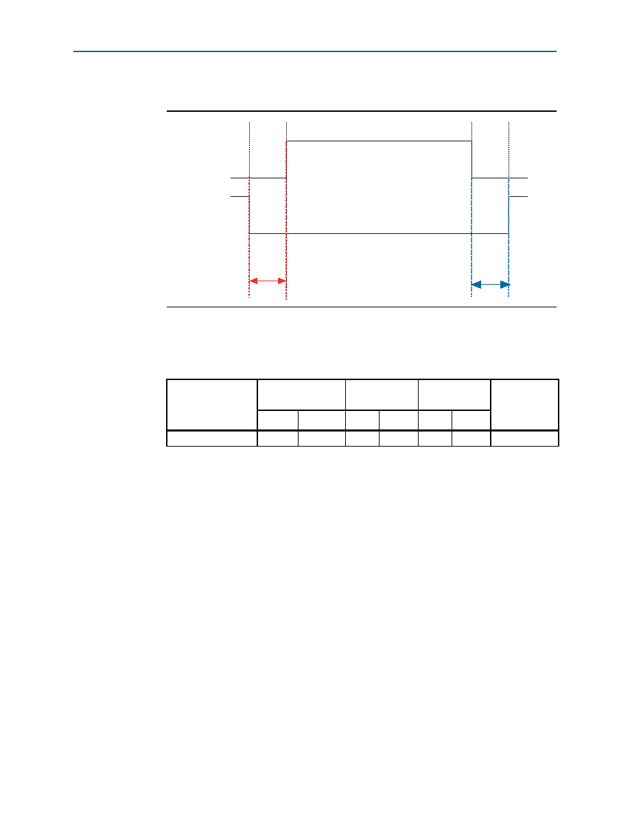
Figure 1–7 shows the timing diagram for the oe and dyn_term_ctrl signals.
Duty Cycle Distortion (DCD) Specifications
Table 1–51 lists the worst-case DCD for Stratix IV devices.
I/O Timing
Altera offers two ways to determine I/O timing—the Excel-based I/O Timing and the
Quartus II Timing Analyzer.
Excel-based I/O Timing provides pin timing performance for each device density and
speed grade. The data is typically used prior to designing the FPGA to get an estimate
of the timing budget as part of the link timing analysis. The Quartus II Timing
Analyzer provides a more accurate and precise I/O timing data based on the specifics
of the design after you complete place-and-route.
f The Excel-based I/O Timing spreadsheet is downloadable from the Literature:
Stratix IV Devices webpage.
Figure 1–7. Timing Diagram for the oe and dyn_term_ctrl Signals
Table 1–51. Worst-Case DCD on Stratix IV I/O Pins (1)
Symbol
–2/–2×
Speed Grade
–3
Speed Grade
–4
Speed Grade
Unit
Min
Max
Min
Max
Min
Max
Output Duty Cycle
45
55
45
55
45
55
%
Note to Table 1–51:
(1) The listed specification is only applicable to the output buffer across different I/O standards.
dyn_term_ctrl
oe
RX
Tristate
TX
TRS_RT
TRS_RT
相关PDF资料 |
PDF描述 |
|---|---|
| 93C56A-I/MS | IC EEPROM 2KBIT 2MHZ 8MSOP |
| EP1S60F1020C6N | IC STRATIX FPGA 60K LE 1020-FBGA |
| A54SX32A-1CQ256 | IC FPGA SX 48K GATES 256-CQFP |
| 93C56A-I/ST | IC EEPROM 2KBIT 2MHZ 8TSSOP |
| EP4SGX110FF35C4N | IC STRATIX IV FPGA 110K 1152FBGA |
相关代理商/技术参数 |
参数描述 |
|---|---|
| EP4SGX110DF29C4N | 功能描述:FPGA - 现场可编程门阵列 FPGA - Stratix IV GX 4224 LABs 372 IOs RoHS:否 制造商:Altera Corporation 系列:Cyclone V E 栅极数量: 逻辑块数量:943 内嵌式块RAM - EBR:1956 kbit 输入/输出端数量:128 最大工作频率:800 MHz 工作电源电压:1.1 V 最大工作温度:+ 70 C 安装风格:SMD/SMT 封装 / 箱体:FBGA-256 |
| EP4SGX110DF29I3 | 功能描述:FPGA - 现场可编程门阵列 FPGA - Stratix IV GX 4224 LABs 372 IOs RoHS:否 制造商:Altera Corporation 系列:Cyclone V E 栅极数量: 逻辑块数量:943 内嵌式块RAM - EBR:1956 kbit 输入/输出端数量:128 最大工作频率:800 MHz 工作电源电压:1.1 V 最大工作温度:+ 70 C 安装风格:SMD/SMT 封装 / 箱体:FBGA-256 |
| EP4SGX110DF29I3N | 功能描述:FPGA - 现场可编程门阵列 FPGA - Stratix IV GX 4224 LABs 372 IOs RoHS:否 制造商:Altera Corporation 系列:Cyclone V E 栅极数量: 逻辑块数量:943 内嵌式块RAM - EBR:1956 kbit 输入/输出端数量:128 最大工作频率:800 MHz 工作电源电压:1.1 V 最大工作温度:+ 70 C 安装风格:SMD/SMT 封装 / 箱体:FBGA-256 |
| EP4SGX110DF29I4 | 功能描述:FPGA - 现场可编程门阵列 FPGA - Stratix IV GX 4224 LABs 372 IOs RoHS:否 制造商:Altera Corporation 系列:Cyclone V E 栅极数量: 逻辑块数量:943 内嵌式块RAM - EBR:1956 kbit 输入/输出端数量:128 最大工作频率:800 MHz 工作电源电压:1.1 V 最大工作温度:+ 70 C 安装风格:SMD/SMT 封装 / 箱体:FBGA-256 |
| EP4SGX110DF29I4N | 功能描述:FPGA - 现场可编程门阵列 FPGA - Stratix IV GX 4224 LABs 372 IOs RoHS:否 制造商:Altera Corporation 系列:Cyclone V E 栅极数量: 逻辑块数量:943 内嵌式块RAM - EBR:1956 kbit 输入/输出端数量:128 最大工作频率:800 MHz 工作电源电压:1.1 V 最大工作温度:+ 70 C 安装风格:SMD/SMT 封装 / 箱体:FBGA-256 |
发布紧急采购,3分钟左右您将得到回复。