参数资料
| 型号: | EP4SGX360FF35C3 |
| 厂商: | Altera |
| 文件页数: | 65/82页 |
| 文件大小: | 0K |
| 描述: | IC STRATIX IV FPGA 360K 1152FBGA |
| 产品培训模块: | Three Reasons to Use FPGA's in Industrial Designs |
| 标准包装: | 3 |
| 系列: | Stratix® IV GX |
| LAB/CLB数: | 14144 |
| 逻辑元件/单元数: | 353600 |
| RAM 位总计: | 23105536 |
| 输入/输出数: | 564 |
| 电源电压: | 0.87 V ~ 0.93 V |
| 安装类型: | 表面贴装 |
| 工作温度: | 0°C ~ 85°C |
| 封装/外壳: | 1152-BBGA |
| 供应商设备封装: | 1152-FBGA(27x27) |
第1页第2页第3页第4页第5页第6页第7页第8页第9页第10页第11页第12页第13页第14页第15页第16页第17页第18页第19页第20页第21页第22页第23页第24页第25页第26页第27页第28页第29页第30页第31页第32页第33页第34页第35页第36页第37页第38页第39页第40页第41页第42页第43页第44页第45页第46页第47页第48页第49页第50页第51页第52页第53页第54页第55页第56页第57页第58页第59页第60页第61页第62页第63页第64页当前第65页第66页第67页第68页第69页第70页第71页第72页第73页第74页第75页第76页第77页第78页第79页第80页第81页第82页
1–60
Chapter 1: DC and Switching Characteristics for Stratix IV Devices
Switching Characteristics
Stratix IV Device Handbook
March 2014
Altera Corporation
Volume 4: Device Datasheet and Addendum
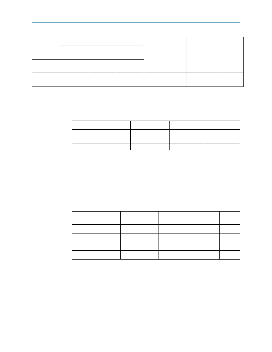
Table 1–47 lists the DQS phase offset delay per stage for Stratix IV devices.
Table 1–48 lists the DQS phase shift error for Stratix IV devices.
4
240-350
240-320
240-290
30°, 60°, 90°, 120°
High
12
5
290-430
290-380
290-360
36°, 72°, 108°, 144°
High
10
6
360-540
360-450
45°, 90°, 135°, 180°
High
8
7
470-700
470-630
470-590
60°, 120°, 180°, 240°
High
6
Note to Table 1–46:
(1) Low indicates a 6-bit DQS delay setting; high indicates a 5-bit DQS delay setting.
Table 1–46. DLL Frequency Range Specifications for Stratix IV Devices (Part 2 of 2)
Frequency
Mode
Frequency Range (MHz)
Available Phase Shift
DQS Delay Buffer
Mode (1)
Number of
Delay
Chains
–2/–2×
Speed Grade
–3
Speed Grade
–4
Speed Grade
Speed Grade
Min
Max
Unit
–2/–2×
7
13
ps
–3
7
15
ps
–4
7
16
ps
Notes to Table 1–47:
(1) The valid settings for phase offset are -64 to +63 for frequency modes 0 to 3 and -32 to +31 for frequency modes
4 to 6.
(2) The typical value equals the average of the minimum and maximum values.
(3) The delay settings are linear, with a cumulative delay variation of 40 ps for all speed grades. For example, when
using a –2 speed grade and applying a 10 phase offset settings to a 90° phase shift at 400 MHz, the expected
average cumulative delay is [625 ps + (10 × 10.5 ps) ± 20 ps] = 730 ps ± 20 ps.
Table 1–48. DQS Phase Shift Error Specification for DLL-Delayed Clock (tDQS_PSERR) for Stratix IV
Devices (1)
Number of DQS Delay
Buffer
–2/–2X
Speed Grade
–3
Speed Grade
–4
Speed Grade
Unit
126
28
30
ps
252
56
60
ps
378
84
90
ps
4
104
112
120
ps
Note to Table 1–48:
(1) This error specification is the absolute maximum and minimum error. For example, skew on three DQS delay
buffers in a –2/–2x speed grade is ± 78 ps or ± 39 ps.
相关PDF资料 |
PDF描述 |
|---|---|
| 93LC66A-E/SN | IC EEPROM 4KBIT 2MHZ 8SOIC |
| EP4SGX290KF40I4 | IC STRATIX IV FPGA 290K 1517FBGA |
| 93LC66CX-E/SN | IC EEPROM 4KBIT 3MHZ 8SOIC |
| EP4SGX290KF40C3 | IC STRATIX IV FPGA 290K 1517FBGA |
| 93LC66AT-E/SN | IC EEPROM 4KBIT 2MHZ 8SOIC |
相关代理商/技术参数 |
参数描述 |
|---|---|
| EP4SGX360FF35C3N | 功能描述:FPGA - 现场可编程门阵列 FPGA - Stratix IV GX 14144 LABs 564 IOs RoHS:否 制造商:Altera Corporation 系列:Cyclone V E 栅极数量: 逻辑块数量:943 内嵌式块RAM - EBR:1956 kbit 输入/输出端数量:128 最大工作频率:800 MHz 工作电源电压:1.1 V 最大工作温度:+ 70 C 安装风格:SMD/SMT 封装 / 箱体:FBGA-256 |
| EP4SGX360FF35C4 | 功能描述:FPGA - 现场可编程门阵列 FPGA - Stratix IV GX 14144 LABs 564 IOs RoHS:否 制造商:Altera Corporation 系列:Cyclone V E 栅极数量: 逻辑块数量:943 内嵌式块RAM - EBR:1956 kbit 输入/输出端数量:128 最大工作频率:800 MHz 工作电源电压:1.1 V 最大工作温度:+ 70 C 安装风格:SMD/SMT 封装 / 箱体:FBGA-256 |
| EP4SGX360FF35C4N | 功能描述:FPGA - 现场可编程门阵列 FPGA - Stratix IV GX 14144 LABs 564 IOs RoHS:否 制造商:Altera Corporation 系列:Cyclone V E 栅极数量: 逻辑块数量:943 内嵌式块RAM - EBR:1956 kbit 输入/输出端数量:128 最大工作频率:800 MHz 工作电源电压:1.1 V 最大工作温度:+ 70 C 安装风格:SMD/SMT 封装 / 箱体:FBGA-256 |
| EP4SGX360FF35I3 | 功能描述:FPGA - 现场可编程门阵列 FPGA - Stratix IV GX 14144 LABs 564 IOs RoHS:否 制造商:Altera Corporation 系列:Cyclone V E 栅极数量: 逻辑块数量:943 内嵌式块RAM - EBR:1956 kbit 输入/输出端数量:128 最大工作频率:800 MHz 工作电源电压:1.1 V 最大工作温度:+ 70 C 安装风格:SMD/SMT 封装 / 箱体:FBGA-256 |
| EP4SGX360FF35I3N | 功能描述:FPGA - 现场可编程门阵列 FPGA - Stratix IV GX 14144 LABs 564 IOs RoHS:否 制造商:Altera Corporation 系列:Cyclone V E 栅极数量: 逻辑块数量:943 内嵌式块RAM - EBR:1956 kbit 输入/输出端数量:128 最大工作频率:800 MHz 工作电源电压:1.1 V 最大工作温度:+ 70 C 安装风格:SMD/SMT 封装 / 箱体:FBGA-256 |
发布紧急采购,3分钟左右您将得到回复。