参数资料
| 型号: | EP4SGX530KH40I4N |
| 厂商: | Altera |
| 文件页数: | 52/82页 |
| 文件大小: | 0K |
| 描述: | IC STRATIX IV FPGA 530K 1517HBGA |
| 产品培训模块: | Three Reasons to Use FPGA's in Industrial Designs |
| 标准包装: | 3 |
| 系列: | Stratix® IV GX |
| LAB/CLB数: | 21248 |
| 逻辑元件/单元数: | 531200 |
| RAM 位总计: | 28033024 |
| 输入/输出数: | 744 |
| 电源电压: | 0.87 V ~ 0.93 V |
| 安装类型: | 表面贴装 |
| 工作温度: | -40°C ~ 100°C |
| 封装/外壳: | 1517-BBGA 裸露焊盘 |
| 供应商设备封装: | 1517-HBGA(42.5x42.5) |
第1页第2页第3页第4页第5页第6页第7页第8页第9页第10页第11页第12页第13页第14页第15页第16页第17页第18页第19页第20页第21页第22页第23页第24页第25页第26页第27页第28页第29页第30页第31页第32页第33页第34页第35页第36页第37页第38页第39页第40页第41页第42页第43页第44页第45页第46页第47页第48页第49页第50页第51页当前第52页第53页第54页第55页第56页第57页第58页第59页第60页第61页第62页第63页第64页第65页第66页第67页第68页第69页第70页第71页第72页第73页第74页第75页第76页第77页第78页第79页第80页第81页第82页
1–48
Chapter 1: DC and Switching Characteristics for Stratix IV Devices
Switching Characteristics
Stratix IV Device Handbook
March 2014
Altera Corporation
Volume 4: Device Datasheet and Addendum
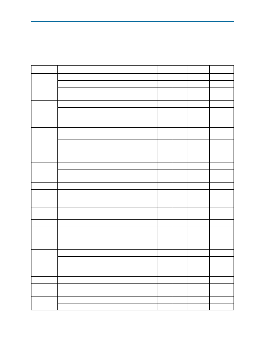
PLL Specifications
Table 1–34 lists the Stratix IV PLL specifications when operating in the commercial
(0° to 85°C), industrial (–40° to 100°C), and military (–55°C to 125°C) junction
temperature ranges.
Table 1–34. PLL Specifications for Stratix IV Devices (Part 1 of 2)
Symbol
Parameter
Min
Typ
Max
Unit
fIN
Input clock frequency (–2/–2x speed grade)
5
—
800 (1)
MHz
Input clock frequency (–3 speed grade)
5
—
717 (1)
MHz
Input clock frequency (–4 speed grade)
5
—
717 (1)
MHz
fINPFD
Input frequency to the PFD
5
—
325
MHz
fVCO (2)
PLL VCO operating range (–2 speed grade)
600
—
1600
MHz
PLL VCO operating range (–3 speed grade)
600
—
1300
MHz
PLL VCO operating range (–4 speed grade)
600
—
1300
MHz
tEINDUTY
Input clock or external feedback clock input duty cycle
40
—
60
%
fOUT
Output frequency for internal global or regional clock
(–2/–2x speed grade)
—
800 (3)
MHz
Output frequency for internal global or regional clock
(–3 speed grade)
—
717 (3)
MHz
Output frequency for internal global or regional clock
(–4 speed grade)
—
717 (3)
MHz
fOUT_EXT
Output frequency for external clock output (–2 speed grade)
—
800 (3)
MHz
Output frequency for external clock output (–3 speed grade)
—
717 (3)
MHz
Output frequency for external clock output (–4 speed grade)
—
717 (3)
MHz
tOUTDUTY
Duty cycle for external clock output (when set to 50%)
45
50
55
%
tFCOMP
External feedback clock compensation time
—
10
ns
tCONFIGPLL
Time required to reconfigure scan chain
—
3.5
—
scanclk
cycles
tCONFIGPHASE
Time required to reconfigure phase shift
—
1
—
scanclk
cycles
fSCANCLK
scanclk frequency
—
100
MHz
tLOCK
Time required to lock from end-of-device configuration or
de-assertion of areset
——
1
ms
tDLOCK
Time required to lock dynamically (after switchover or
reconfiguring any non-post-scale counters/delays)
——
1
ms
fCLBW
PLL closed-loop low bandwidth
—
0.3
—
MHz
PLL closed-loop medium bandwidth
—
1.5
—
MHz
PLL closed-loop high bandwidth (8)
—4
—
MHz
tPLL_PSERR
Accuracy of PLL phase shift
—
±50
ps
tARESET
Minimum pulse width on the areset signal
10
—
ns
Input clock cycle to cycle jitter (FREF ≥ 100 MHz)
—
0.15
UI (p-p)
Input clock cycle to cycle jitter (FREF < 100 MHz)
—
±750
ps (p-p)
tOUTPJ_DC (6)
Period Jitter for dedicated clock output (FOUT ≥ 100 MHz)
—
175
ps (p-p)
Period Jitter for dedicated clock output (FOUT < 100 MHz)
—
17.5
mUI (p-p)
相关PDF资料 |
PDF描述 |
|---|---|
| EP4SGX530KF43I4N | IC STRATIX IV FPGA 530K 1760FBGA |
| 93C46AT-E/MNY | IC EEPROM SER 1K 1.8V 8TDFN |
| 93LC46BT-E/MNY | IC EEPROM SER 1K 2.5V 8TDFN |
| EP4SGX530KH40C3N | IC STRATIX IV GX 530K 1517HBGA |
| 24LC025T-E/SN | IC EEPROM 2KBIT 400KHZ 8SOIC |
相关代理商/技术参数 |
参数描述 |
|---|---|
| EP4SGX530NF45C2 | 功能描述:FPGA - 现场可编程门阵列 FPGA - Stratix IV GX 21248 LABs 920 IOs RoHS:否 制造商:Altera Corporation 系列:Cyclone V E 栅极数量: 逻辑块数量:943 内嵌式块RAM - EBR:1956 kbit 输入/输出端数量:128 最大工作频率:800 MHz 工作电源电压:1.1 V 最大工作温度:+ 70 C 安装风格:SMD/SMT 封装 / 箱体:FBGA-256 |
| EP4SGX530NF45C2ES | 制造商:Altera Corporation 功能描述:FPGA Stratix 制造商:Altera Corporation 功能描述:IC STRATIX IV FPGA |
| EP4SGX530NF45C2N | 功能描述:FPGA - 现场可编程门阵列 FPGA - Stratix IV GX 21248 LABs 920 IOs RoHS:否 制造商:Altera Corporation 系列:Cyclone V E 栅极数量: 逻辑块数量:943 内嵌式块RAM - EBR:1956 kbit 输入/输出端数量:128 最大工作频率:800 MHz 工作电源电压:1.1 V 最大工作温度:+ 70 C 安装风格:SMD/SMT 封装 / 箱体:FBGA-256 |
| EP4SGX530NF45C2NES | 制造商:Altera Corporation 功能描述:FPGA Stratix |
| EP4SGX530NF45C3 | 功能描述:FPGA - 现场可编程门阵列 FPGA - Stratix IV GX 21248 LABs 920 IOs RoHS:否 制造商:Altera Corporation 系列:Cyclone V E 栅极数量: 逻辑块数量:943 内嵌式块RAM - EBR:1956 kbit 输入/输出端数量:128 最大工作频率:800 MHz 工作电源电压:1.1 V 最大工作温度:+ 70 C 安装风格:SMD/SMT 封装 / 箱体:FBGA-256 |
发布紧急采购,3分钟左右您将得到回复。