- 您现在的位置:买卖IC网 > PDF目录22010 > EPF10K20TI144-4N (Altera)IC FLEX 10K FPGA 20K 144-TQFP PDF资料下载
参数资料
| 型号: | EPF10K20TI144-4N |
| 厂商: | Altera |
| 文件页数: | 25/128页 |
| 文件大小: | 0K |
| 描述: | IC FLEX 10K FPGA 20K 144-TQFP |
| 产品培训模块: | Three Reasons to Use FPGA's in Industrial Designs |
| 标准包装: | 60 |
| 系列: | FLEX-10K® |
| LAB/CLB数: | 144 |
| 逻辑元件/单元数: | 1152 |
| RAM 位总计: | 12288 |
| 输入/输出数: | 102 |
| 门数: | 63000 |
| 电源电压: | 4.5 V ~ 5.5 V |
| 安装类型: | 表面贴装 |
| 工作温度: | -40°C ~ 100°C |
| 封装/外壳: | 144-LQFP |
| 供应商设备封装: | 144-TQFP(20x20) |
| 其它名称: | 544-2221 |
第1页第2页第3页第4页第5页第6页第7页第8页第9页第10页第11页第12页第13页第14页第15页第16页第17页第18页第19页第20页第21页第22页第23页第24页当前第25页第26页第27页第28页第29页第30页第31页第32页第33页第34页第35页第36页第37页第38页第39页第40页第41页第42页第43页第44页第45页第46页第47页第48页第49页第50页第51页第52页第53页第54页第55页第56页第57页第58页第59页第60页第61页第62页第63页第64页第65页第66页第67页第68页第69页第70页第71页第72页第73页第74页第75页第76页第77页第78页第79页第80页第81页第82页第83页第84页第85页第86页第87页第88页第89页第90页第91页第92页第93页第94页第95页第96页第97页第98页第99页第100页第101页第102页第103页第104页第105页第106页第107页第108页第109页第110页第111页第112页第113页第114页第115页第116页第117页第118页第119页第120页第121页第122页第123页第124页第125页第126页第127页第128页
120
Altera Corporation
FLEX 10K Embedded Programmable Logic Device Family Data Sheet
Notes:
(1)
To implement the ClockLock and ClockBoost circuitry with the MAX+PLUS II software, designers must specify the
input frequency. The MAX+PLUS II software tunes the PLL in the ClockLock and ClockBoost circuitry to this
frequency. The fCLKDEV parameter specifies how much the incoming clock can differ from the specified frequency
during device operation. Simulation does not reflect this parameter.
(2)
During device configuration, the ClockLock and ClockBoost circuitry is configured before the rest of the device. If
the incoming clock is supplied during configuration, the ClockLock and ClockBoost circuitry locks during
configuration, because the tLOCK value is less than the time required for configuration.
(3)
The tJITTER specification is measured under long-term observation.
Power
Consumption
The supply power (P) for FLEX 10K devices can be calculated with the
following equation:
P = PINT + PIO = (ICCSTANDBY + ICCACTIVE) × VCC + PIO
Typical ICCSTANDBY values are shown as ICC0 in the FLEX 10K device DC
ICCACTIVE value depends on the switching frequency and the application
logic. This value is calculated based on the amount of current that each LE
typically consumes. The PIO value, which depends on the device output
load characteristics and switching frequency, can be calculated using the
guidelines given in Application Note 74 (Evaluating Power for Altera Devices).
1
Compared to the rest of the device, the embedded array
consumes a negligible amount of power. Therefore, the
embedded array can be ignored when calculating supply
current.
The ICCACTIVE value is calculated with the following equation:
ICCACTIVE = K × fMAX × N × togLC ×
The parameters in this equation are shown below:
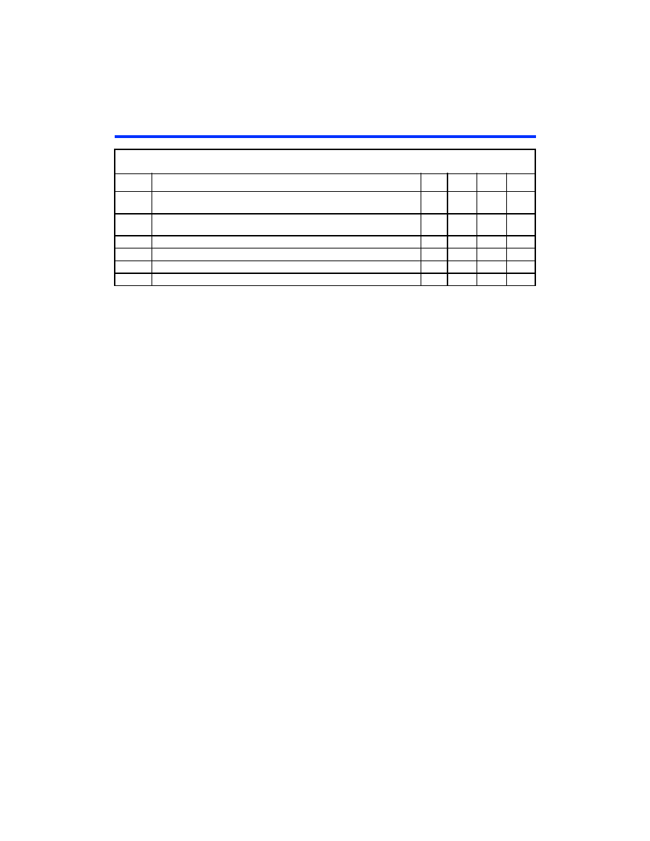
fCLKDEV1 Input deviation from user specification in MAX+PLUS II (ClockBoost clock
multiplication factor equals 1) (1)
±1MHz
fCLKDEV2 Input deviation from user specification in MAX+PLUS II (ClockBoost clock
multiplication factor equals 2) (1)
±0.5
MHz
tINCLKSTB Input clock stability (measured between adjacent clocks)
100
ps
tLOCK
Time required for ClockLock or ClockBoost to acquire lock (2)
10
s
tJITTER
Jitter on ClockLock or ClockBoost-generated clock (3)
1ns
tOUTDUTY Duty cycle for ClockLock or ClockBoost-generated clock
40
50
60
%
Table 113. ClockLock & ClockBoost Parameters
(Part 2 of 2)
Symbol
Parameter
Min
Typ
Max
Unit
A
MHz
LE
×
---------------------------
相关PDF资料 |
PDF描述 |
|---|---|
| RSC44DRYH-S13 | CONN EDGECARD 88POS .100 EXTEND |
| RMC44DRYH-S13 | CONN EDGECARD 88POS .100 EXTEND |
| EPF10K20TI144-4 | IC FLEX 10K FPGA 20K 144-TQFP |
| RSC60DREN | CONN EDGECARD 120POS .100 EYELET |
| A54SX32A-TQG144 | IC FPGA 249I/O 144TQFP |
相关代理商/技术参数 |
参数描述 |
|---|---|
| EPF10K250A | 制造商:ALTERA 制造商全称:Altera Corporation 功能描述:Embedded Programmable Logic Device Family |
| EPF10K250ABC600-2 | 制造商:Rochester Electronics LLC 功能描述:- Bulk |
| EPF10K250AGC599-1 | 制造商:Rochester Electronics LLC 功能描述:- Bulk 制造商:Altera Corporation 功能描述: |
| EPF10K250AGC599-2 | 制造商:Rochester Electronics LLC 功能描述:- Bulk |
| EPF10K250AGC599-3 | 制造商:Rochester Electronics LLC 功能描述:- Bulk |
发布紧急采购,3分钟左右您将得到回复。