- 您现在的位置:买卖IC网 > PDF目录362754 > EPVP6300 (ELAN Microelctronics Corp .) VFD Controller PDF资料下载
参数资料
| 型号: | EPVP6300 |
| 厂商: | ELAN Microelctronics Corp . |
| 英文描述: | VFD Controller |
| 中文描述: | 变频控制器 |
| 文件页数: | 12/63页 |
| 文件大小: | 517K |
| 代理商: | EPVP6300 |
第1页第2页第3页第4页第5页第6页第7页第8页第9页第10页第11页当前第12页第13页第14页第15页第16页第17页第18页第19页第20页第21页第22页第23页第24页第25页第26页第27页第28页第29页第30页第31页第32页第33页第34页第35页第36页第37页第38页第39页第40页第41页第42页第43页第44页第45页第46页第47页第48页第49页第50页第51页第52页第53页第54页第55页第56页第57页第58页第59页第60页第61页第62页第63页
ePVP6300
VFD Controller
6 of 63
11.04.2004
(V1.92)
This specification is subject to change without further notice.
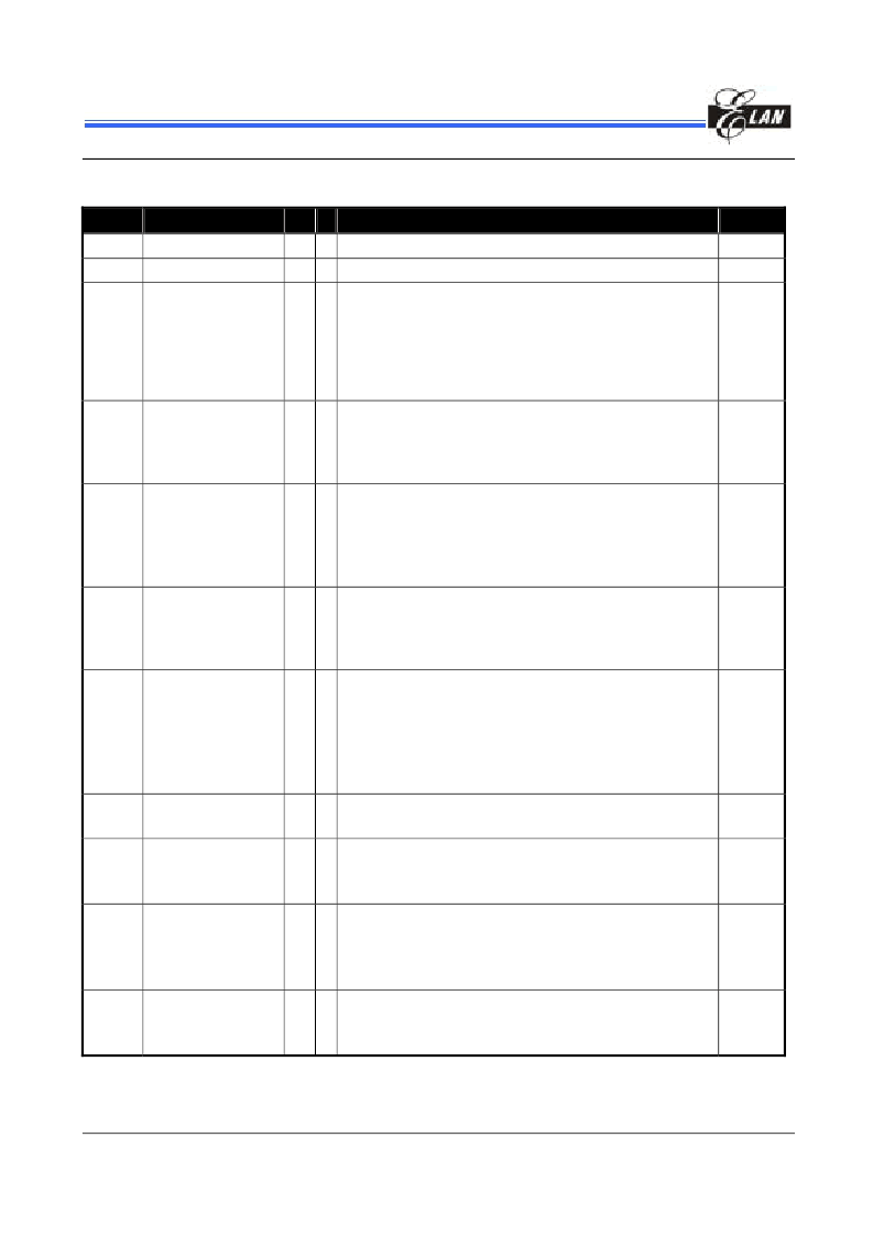
6 Pin Descriptions
Pin No.
Pin Name
I/O #
Description
Note
61,62
NC
2
13,14
VDD
-
2 Logic power supply
57
STB/GPIOC4
I/O 1
1. Serial Interface Strobe input pin. While the STB goes low, it
will cause interrupt event. The data input after the STB has
fallen is processed as a command. When this pin is “HIGH,”
CLK is ignored.
2. Programmable Internal pull high
3. GPIOC4 function
Schmitt
Pull-up
58
CLK/GPIOC5
I/O 1
1. Clock input pin. This pin reads serial data at the rising edge
and outputs data at the falling edge.
2. Programmable Internal pull high
3. GPIOC5 function
Schmitt
Pull-up
59
DOUT/GPIOC6
I/O 1
1. Data output pin (N-channel, Open-Drain)
2. This pin outputs serial data at the falling edge of the shift clock
(starting from lower bit).
3. Programmable internal pull high
4. GPIOC6 function
Schmitt
Pull-up
60
DIN/GPIOC7
I/O 1
1. Data input pin. This pin inputs serial data at the rising edge of
the shift clock (starting from lower bit.)
2. Programmable Internal pull high
3. GPIOC7 function
Schmitt
Pull-up
53 – 54
GPIOC0 – GPIOC3
I/O 4
General Purpose I/O pins
:
1. Key data input to these pins is latched at the end of display
cycle.
2. These pins constitute 4-bit general-purpose input/output port.
3. Programmable Internal Pull-High
4. Wake-up Function
Schmitt
Pull-up
15-22
(B Cell)
GR1 – GR8
O
8
1. High voltage grid output
2. High breakdown output
~
23-30
(B Cell)
GR9/P9/SG20
–
GR16/ SG13
O
8
1. High voltage grid output
2. High breakdown output
3. High voltage segment output
31-33
(B Cell)
GR17/SG12/KS12
–
GR19 /SG10/KS10
O
3
1. High voltage grid output
2. High breakdown output
3. High voltage segment output
4. Matrix key scan output
34-38
(A Cell)
SG9/KS9
–
SG5/KS5
O
5
1. High breakdown output
2. High voltage segment output
3. Matrix key scan output
相关PDF资料 |
PDF描述 |
|---|---|
| EPVP6800 | VFD Controller |
| EPVP6810 | VFD Controller |
| EPXA4 | Excalibur Devices |
| EPZ3001G | Power Choke |
| EPZ3003G | Power Choke |
相关代理商/技术参数 |
参数描述 |
|---|---|
| EPVP6800 | 制造商:EMC 制造商全称:ELAN Microelectronics Corp 功能描述:VFD Controller |
| EPVP6810 | 制造商:EMC 制造商全称:ELAN Microelectronics Corp 功能描述:VFD Controller |
| EPWB400 | 制造商:Electrolube 功能描述:PAINT, WHITE GLOSS 400ML |
| EPWR30 | 制造商:Black Box Corporation 功能描述:ALL-WEATHER SINGLE OUTLETORANG |
| EPWR32 | 制造商:Black Box Corporation 功能描述:ALL-WEATHER SINGLE OUTLETORANG |
发布紧急采购,3分钟左右您将得到回复。