- 您现在的位置:买卖IC网 > PDF目录362754 > EPVP6800 (ELAN Microelctronics Corp .) VFD Controller PDF资料下载
参数资料
| 型号: | EPVP6800 |
| 厂商: | ELAN Microelctronics Corp . |
| 英文描述: | VFD Controller |
| 中文描述: | 变频控制器 |
| 文件页数: | 17/47页 |
| 文件大小: | 325K |
| 代理商: | EPVP6800 |
第1页第2页第3页第4页第5页第6页第7页第8页第9页第10页第11页第12页第13页第14页第15页第16页当前第17页第18页第19页第20页第21页第22页第23页第24页第25页第26页第27页第28页第29页第30页第31页第32页第33页第34页第35页第36页第37页第38页第39页第40页第41页第42页第43页第44页第45页第46页第47页
ePVP6800
VFD Controller
This specification is subject to change without further notice.
11.28.2004 (V123)
11 of 47
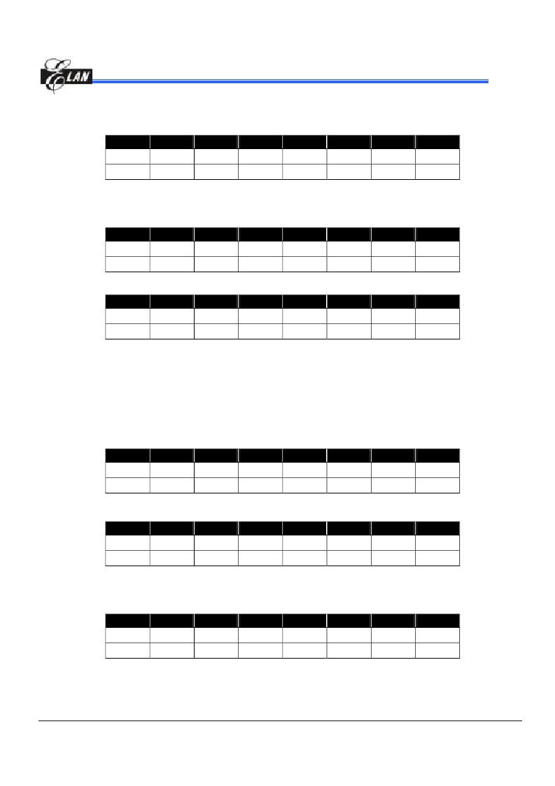
7.2.7 R6 (PORT6 Output Data, SPI Data Buffer)
a) PAGE 0 (PORT6 Output Data Register for HV)
Bit 7
Bit 6
Bit 5
Bit 4
Bit 3
Bit 2
Bit 1
Bit 0
P67
P66
P65
P64
P63
P62
P61
P60
W-0
W-0
W-0
W-0
W-0
W-0
W-0
W-0
7.2.8 R7 (PORT7 Output Data, Counter1 Data
a) PAGE 0 (PORT7 Output Data Register for HV)
Bit 7
Bit 6
Bit 5
Bit 4
Bit 3
Bit 2
Bit 1
Bit 0
P77
P76
P75
P74
P73
P72
P71
P70
W-0
W-0
W-0
W-0
W-0
W-0
W-0
W-0
c) PAGE 2 (Counter 1 Data Register)
Bit 7
Bit 6
Bit 5
Bit 4
Bit 3
Bit 2
Bit 1
Bit 0
CN17
CN16
CN15
CN14
CN13
CN12
CN11
CN10
R/W-0
R/W-0
R/W-0
R/W-0
R/W-0
R/W-0
R/W-0
R/W-0
Bit 0 ~ Bit 7 (CN10 ~ CN17)
:
Counter1 buffer that you can read and write.
Counter1 is an 8-bit up-counter with 8-bit prescaler that allows you to
use R7 PAGE2 to preset and read the counter (write
preset). After
an interruption, it will reload the preset value.
7.2.9 R8 (PORT8 Output data, Data RAM address) , Counter2_LB data
a) PAGE 0 (PORT8 Output Data Register for HV)
Bit 7
Bit 6
Bit 5
Bit 4
Bit 3
Bit 2
Bit 1
Bit 0
P87
P86
P85
P84
P83
P82
P81
P80
W-0
W-0
W-0
W-0
W-0
W-0
W-0
W-0
b) PAGE 1 (Data RAM Address Register)
Bit 7
Bit 6
Bit 5
Bit 4
Bit 3
Bit 2
Bit 1
Bit 0
RAM_A7
RAM_A6
RAM_A5
RAM_A4
RAM_A3
RAM_A2
RAM_A1
RAM_A0
R/W-0
R/W-0
R/W-0
R/W-0
R/W-0
R/W-0
R/W-0
R/W-0
Bit 0 ~ Bit 7 (RAM_A0 ~ RAM_A7)
:
data RAM address
c) PAGE 2 (Counter2 Low Byte Data Register)
Bit 7
Bit 6
Bit 5
Bit 4
Bit 3
Bit 2
Bit 1
Bit 0
CN27
CN26
CN25
CN24
CN23
CN22
CN21
CN20
R/W
R/W
R/W
R/W
R/W
R/W
R/W
R/W
Bit 0 ~ Bit 7 (CN20 ~ CN27)
:
Counter2_LB's buffer that you can read and write.
Counter2 is a 16-bit up-counter with 8-bit prescaler that allows you to
use R8 PAGE2 to preset and read the counter.(write
preset). After
an interruption, it will reload the preset value.
相关PDF资料 |
PDF描述 |
|---|---|
| EPVP6810 | VFD Controller |
| EPXA4 | Excalibur Devices |
| EPZ3001G | Power Choke |
| EPZ3003G | Power Choke |
| EPZ3006G | Power Choke |
相关代理商/技术参数 |
参数描述 |
|---|---|
| EPVP6810 | 制造商:EMC 制造商全称:ELAN Microelectronics Corp 功能描述:VFD Controller |
| EPWB400 | 制造商:Electrolube 功能描述:PAINT, WHITE GLOSS 400ML |
| EPWR30 | 制造商:Black Box Corporation 功能描述:ALL-WEATHER SINGLE OUTLETORANG |
| EPWR32 | 制造商:Black Box Corporation 功能描述:ALL-WEATHER SINGLE OUTLETORANG |
| EPWR40 | 制造商:Black Box Corporation 功能描述:Power Outlet Strip |
发布紧急采购,3分钟左右您将得到回复。