- 您现在的位置:买卖IC网 > PDF目录16231 > EVAL-AD5252EBZ (Analog Devices Inc)BOARD EVAL FOR AD5252 PDF资料下载
参数资料
| 型号: | EVAL-AD5252EBZ |
| 厂商: | Analog Devices Inc |
| 文件页数: | 15/28页 |
| 文件大小: | 0K |
| 描述: | BOARD EVAL FOR AD5252 |
| 标准包装: | 1 |
| 主要目的: | 数字电位器 |
| 已用 IC / 零件: | AD5252 |
| 主要属性: | 2 通道,256 位置 |
| 次要属性: | I²C 接口 |
| 已供物品: | 板 |
第1页第2页第3页第4页第5页第6页第7页第8页第9页第10页第11页第12页第13页第14页当前第15页第16页第17页第18页第19页第20页第21页第22页第23页第24页第25页第26页第27页第28页
AD5251/AD5252
Data Sheet
Rev. D | Page 22 of 28
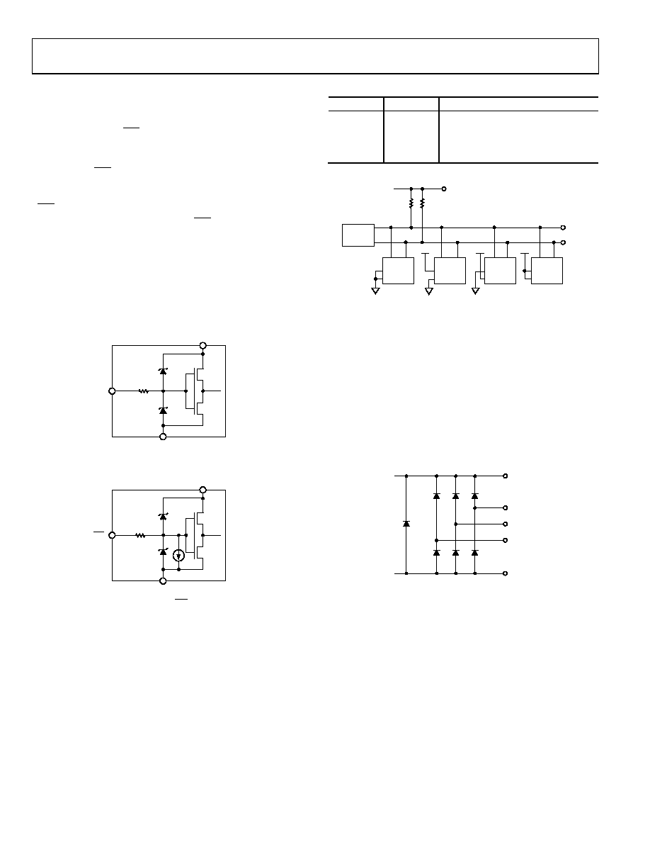
DIGITAL INPUT/OUTPUT CONFIGURATION
SDA is a digital input/output with an open-drain MOSFET that
requires a pull-up resistor for proper communication. On the
other hand, SCL and WP are digital inputs for which pull-up
resistors are recommended to minimize the MOSFET cross-
conduction current when the driving signals are lower than
VDD. SCL and WP have ESD protection diodes, as shown in
Figure 35 and Figure 36.
WP can be permanently tied to VDD without a pull-up resistor if
the write-protect feature is not used. If WP is left floating, an
internal current source pulls it low to enable write protection. In
applications in which the device is programmed infrequently,
this allows the part to default to write-protection mode after
any one-time factory programming or field calibration without
using an on-board pull-down resistor. Because there are
protection diodes on all inputs, the signal levels must not be
greater than VDD to prevent forward biasing of the diodes.
03823-0-035
GND
SCL
VDD
Figure 35. SCL Digital Input
03823-0-036
GND
INPUTS
WP
VDD
Figure 36. Equivalent WP Digital Input
MULTIPLE DEVICES ON ONE BUS
The AD5251/AD5252 are equipped with two addressing pins,
AD1 and AD0, that allow up to four AD5251/AD5252 devices
to be operated on one I2C bus. To achieve this result, the states of
AD1 and AD0 on each device must first be defined. An example
device is issued a different slave address—01011(AD1)(AD0)—
to complete the addressing.
Table 12. Multiple Devices Addressing
AD1
AD0
Device Addressed
0
U1
0
1
U2
1
0
U3
1
U4
03823-0-037
5V
RP
5V
U1
AD0
AD1
SDA SCL
MASTER
U2
AD0
AD1
SDA SCL
U3
AD0
AD1
SDA SCL
U4
AD0
AD1
SDA
SCL
Figure 37. Multiple AD5251/AD5252 Devices on a Single Bus
TERMINAL VOLTAGE OPERATION RANGE
The AD5251/AD5252 are designed with internal ESD diodes
for protection; these diodes also set the boundaries for the
terminal operating voltages. Positive signals present on
Terminal A, Terminal B, or Terminal W that exceed VDD are
clamped by the forward-biased diode. Similarly, negative signals
on Terminal A, Terminal B, or Terminal W that are more
users should not operate VAB, VWA, and VWB to be higher than
the voltage across VDD to VSS, but VAB, VWA, and VWB have no
polarity constraint.
VSS
VDD
A
W
B
03823-0-018
Figure 38. Maximum Terminal Voltages Set by VDD and VSS
POWER-UP AND POWER-DOWN SEQUENCES
Because the ESD protection diodes limit the voltage compliance
at Terminal A, Terminal B, and Terminal W (see Figure 38), it is
important to power on VDD/VSS before applying any voltage to
these terminals. Otherwise, the diodes are forward biased such
that VDD/VSS are powered unintentionally and may affect the
user’s circuit. Similarly, VDD/VSS should be powered down last.
The ideal power-up sequence is in the following order: GND,
VDD, VSS, digital inputs, and VA/VB/VW. The order of powering
VA, VB, VW, and the digital inputs is not important, as long as
they are powered after VDD/VSS.
相关PDF资料 |
PDF描述 |
|---|---|
| 101-0452 | KIT DEV RABBIT RCM2100 INTL |
| VE-J7X-EZ-F1 | CONVERTER MOD DC/DC 5.2V 25W |
| EVAL-ADF4360-8EBZ1 | BOARD EVALUATION FOR ADF4360-8 |
| VE-J7X-EY-S | CONVERTER MOD DC/DC 5.2V 50W |
| MCP73213-B6SI/MF | IC LI-ION/LI-POLY CTRLR 10-DFN |
相关代理商/技术参数 |
参数描述 |
|---|---|
| EVAL-AD5252SDZ | 功能描述:BOARD EVAL FOR AD5252 RoHS:是 类别:编程器,开发系统 >> 评估演示板和套件 系列:- 标准包装:1 系列:- 主要目的:电信,线路接口单元(LIU) 嵌入式:- 已用 IC / 零件:IDT82V2081 主要属性:T1/J1/E1 LIU 次要属性:- 已供物品:板,电源,线缆,CD 其它名称:82EBV2081 |
| EVAL-AD5254EBZ | 制造商:Analog Devices 功能描述:EVALUATION BOARD - Boxed Product (Development Kits) |
| EVAL-AD5254SDZ | 功能描述:BOARD EVAL FOR AD5254 RoHS:是 类别:编程器,开发系统 >> 评估演示板和套件 系列:- 标准包装:1 系列:- 主要目的:电信,线路接口单元(LIU) 嵌入式:- 已用 IC / 零件:IDT82V2081 主要属性:T1/J1/E1 LIU 次要属性:- 已供物品:板,电源,线缆,CD 其它名称:82EBV2081 |
| EVAL-AD5258DBZ | 功能描述:BOARD EVAL FOR AD5258DBZ RoHS:否 类别:编程器,开发系统 >> 评估演示板和套件 系列:* 标准包装:1 系列:- 主要目的:电信,线路接口单元(LIU) 嵌入式:- 已用 IC / 零件:IDT82V2081 主要属性:T1/J1/E1 LIU 次要属性:- 已供物品:板,电源,线缆,CD 其它名称:82EBV2081 |
| EVAL-AD5259DBZ | 功能描述:BOARD EVAL FOR AD5259DBZ RoHS:否 类别:编程器,开发系统 >> 评估演示板和套件 系列:* 标准包装:1 系列:- 主要目的:电信,线路接口单元(LIU) 嵌入式:- 已用 IC / 零件:IDT82V2081 主要属性:T1/J1/E1 LIU 次要属性:- 已供物品:板,电源,线缆,CD 其它名称:82EBV2081 |
发布紧急采购,3分钟左右您将得到回复。