- 您现在的位置:买卖IC网 > PDF目录16581 > EVAL-AD5273DBZ (Analog Devices Inc)BOARD EVAL FOR AD5273DBZ PDF资料下载
参数资料
| 型号: | EVAL-AD5273DBZ |
| 厂商: | Analog Devices Inc |
| 文件页数: | 11/24页 |
| 文件大小: | 0K |
| 描述: | BOARD EVAL FOR AD5273DBZ |
| 标准包装: | 1 |
| 系列: | * |
AD5273
Rev. H | Page 19 of 24
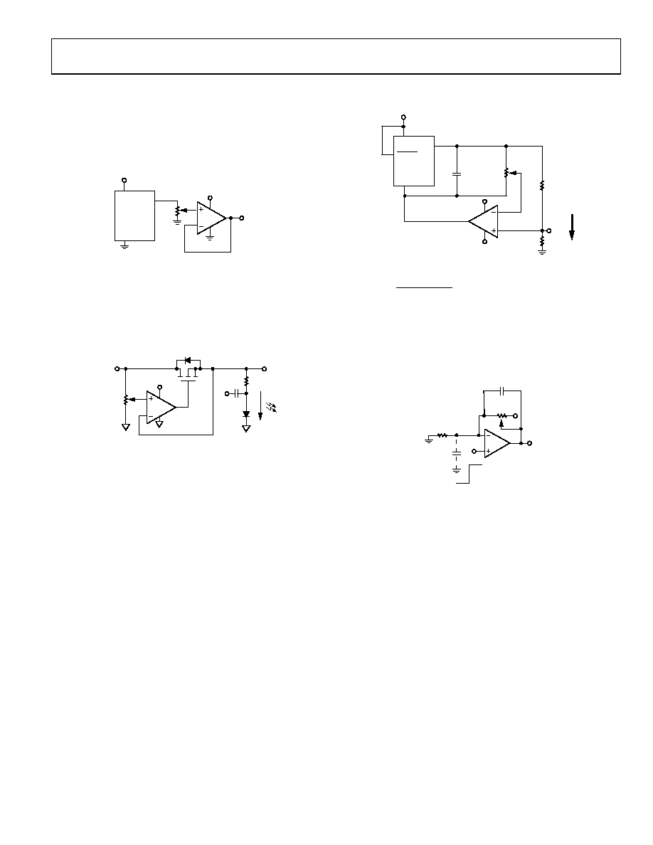
APPLICATIONS INFORMATION
DAC
It is common to buffer the output of the digital potentiometer as
a DAC. The buffer minimizes the load dependence and delivers
higher current to the load, if needed.
GND
VIN
VOUT
1U1
5V
2
3
VO
AD8601
5V
A
W
B
ADR03
U3
AD5273
U2
03224-046
Figure 46. Programmable Voltage Reference (DAC)
PROGRAMMABLE VOLTAGE SOURCE WITH
BOOSTED OUTPUT
For applications that require high current adjustment, such as a
laser diode driver or tunable laser, consider a booster voltage
source, as shown in Figure 47.
+V
W
SIGNAL
CC
RBIAS
LD
VIN
A
B
VOUT
U1
AD5273
U3 2N7002
AD8601
U2
–V
IL
03
22
4-
04
7
Figure 47. Programmable Booster Voltage Source
In this circuit, the inverting input of the op amp forces the
VOUT to be equal to the wiper voltage set by the digital potenti-
ometer. The load current is then delivered by the supply via the
N-Channel FET, N1. N1 power handling must be adequate to
dissipate (VIN VOUT) × IL power. This circuit can source a max-
imum of 100 mA with a 5 V supply. For precision applications,
can be applied at Terminal A of the digital potentiometer.
PROGRAMMABLE CURRENT SOURCE
A programmable current source can be implemented with the
circuit shown in Figure 48. The load current is the voltage across
Terminal B to Terminal W of the AD5273 divided by RS. At zero
scale, Terminal A of the AD5273 is 2.048 V, which makes the
wiper voltage clamped at ground potential. Depending on the
load, Equation 5 is therefore valid only at certain codes. For
example, when the compliance voltage, VL, equals half of VREF,
the current can be programmed from midscale to full scale of
the AD5273.
IL
GND
VS
2U1
5V
4
6
3
SLEEP
0V TO ...
OUPUT
REF191
C1
1F
B
A
W
RS
102
100
RL
VL
–2.048 + VL
–5V
OP1177
+5V
V+
V–
U2
U3
AD5273
03
224
-04
8
Figure 48. Programmable Current Source
(
)
63
32
|
64
/
≤
×
=
D
R
D
V
I
S
REF
L
(5)
GAIN CONTROL COMPENSATION
As shown in Figure 49, the digital potentiometers are
commonly used in gain controls or sensor transimpedance
amplifier signal conditioning applications.
U1
C2
4.7pF
A
B
W
VO
VI
C1
R1
47k
Ω
R2
100k
Ω
03224-049
Figure 49. Typical Noninverting Gain Amplifier
In both applications, one of the digital potentiometer terminals
is connected to the op amp inverting node with finite terminal
capacitance, C1. It introduces a zero for the 1 βo term with
20 dB/dec, whereas a typical op amp GBP has 20 dB/dec
characteristics. A large R2 and finite C1 can cause this zero’s
frequency to fall well below the crossover frequency. Therefore,
the rate of closure becomes 40 dB/dec and the system has a 0°
phase margin at the crossover frequency. The output may ring,
or in the worst case, oscillate when the input is a step function.
Similarly, it is also likely to ring when switching between two
gain values because this is equivalent to a step change at the
input. To reduce the effect of C1, users should also configure
Terminal B or Terminal A rather than Terminal W at the
inverting node.
相关PDF资料 |
PDF描述 |
|---|---|
| ECM28DCAN-S189 | CONN EDGECARD 56POS R/A .156 SLD |
| H3CCH-6406M | IDC CABLE - HKC64H/AE64M/HKC64H |
| ECM28DCAH-S189 | CONN EDGECARD 56POS R/A .156 SLD |
| MC3PHACVDWE | IC MOTOR CONTROLLER 28-SOIC |
| MAX8890ETCABK+T | IC POWER MANAGE CELL 12-TQFN |
相关代理商/技术参数 |
参数描述 |
|---|---|
| EVAL-AD5282EBZ | 功能描述:BOARD EVALUATION FOR AD5282 RoHS:是 类别:编程器,开发系统 >> 评估演示板和套件 系列:- 标准包装:1 系列:- 主要目的:电信,线路接口单元(LIU) 嵌入式:- 已用 IC / 零件:IDT82V2081 主要属性:T1/J1/E1 LIU 次要属性:- 已供物品:板,电源,线缆,CD 其它名称:82EBV2081 |
| EVAL-AD5290EBZ | 功能描述:BOARD EVAL FOR AD5290 RoHS:是 类别:编程器,开发系统 >> 评估演示板和套件 系列:- 标准包装:1 系列:- 主要目的:电信,线路接口单元(LIU) 嵌入式:- 已用 IC / 零件:IDT82V2081 主要属性:T1/J1/E1 LIU 次要属性:- 已供物品:板,电源,线缆,CD 其它名称:82EBV2081 |
| EVAL-AD5292EBZ | 功能描述:BOARD EVAL FOR AD5292 RoHS:是 类别:编程器,开发系统 >> 评估演示板和套件 系列:- 标准包装:1 系列:- 主要目的:电信,线路接口单元(LIU) 嵌入式:- 已用 IC / 零件:IDT82V2081 主要属性:T1/J1/E1 LIU 次要属性:- 已供物品:板,电源,线缆,CD 其它名称:82EBV2081 |
| EVAL-AD5360EBZ | 功能描述:BOARD EVAL FOR AD5360 RoHS:是 类别:编程器,开发系统 >> 评估板 - 数模转换器 (DAC) 系列:- 产品培训模块:Lead (SnPb) Finish for COTS Obsolescence Mitigation Program 标准包装:1 系列:- DAC 的数量:4 位数:12 采样率(每秒):- 数据接口:串行,SPI? 设置时间:3µs DAC 型:电流/电压 工作温度:-40°C ~ 85°C 已供物品:板 已用 IC / 零件:MAX5581 |
| EVAL-AD5360EBZ1 | 制造商:AD 制造商全称:Analog Devices 功能描述:16-Channel, 16-/14-Bit, Serial Input, Voltage-Output DAC |
发布紧急采购,3分钟左右您将得到回复。