- 您现在的位置:买卖IC网 > PDF目录17075 > EVAL-AD5373EBZ (Analog Devices Inc)BOARD EVAL FOR AD5373 PDF资料下载
参数资料
| 型号: | EVAL-AD5373EBZ |
| 厂商: | Analog Devices Inc |
| 文件页数: | 3/29页 |
| 文件大小: | 0K |
| 描述: | BOARD EVAL FOR AD5373 |
| 产品培训模块: | DAC Architectures |
| 标准包装: | 1 |
| DAC 的数量: | 32 |
| 位数: | 14 |
| 采样率(每秒): | 540k |
| 数据接口: | 串行 |
| 设置时间: | 20µs |
| DAC 型: | 电压 |
| 工作温度: | -40°C ~ 85°C |
| 已供物品: | 板,CD |
| 已用 IC / 零件: | AD5373 |
第1页第2页当前第3页第4页第5页第6页第7页第8页第9页第10页第11页第12页第13页第14页第15页第16页第17页第18页第19页第20页第21页第22页第23页第24页第25页第26页第27页第28页第29页
AD5372/AD5373
Rev. C | Page 10 of 28
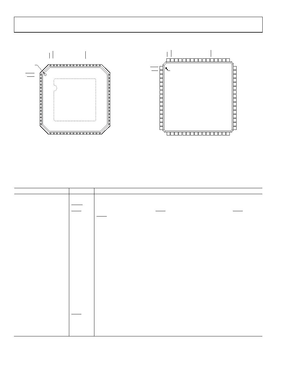
PIN CONFIGURATIONS AND FUNCTION DESCRIPTIONS
VOUT27
SIGGND3
VOUT28
VOUT29
VOUT30
VOUT31
NC
VDD
BUSY
RESET
SIGGND0
VOUT3
VOUT2
VOUT1
VOUT0
VREF0
VOUT23
VOUT22
VOUT21
VSS
VOUT20
VDD
SIGGND2
VOUT19
VOUT4
VOUT5
VO
U
T
26
VO
U
T
25
VO
U
T
24
AG
N
D
DG
N
D
DV
CC
SD
O
SD
I
SC
L
K
DV
CC
DG
N
D
VO
U
T
7
VO
U
T
6
NC
VO
U
T
8
VO
U
T
9
VO
U
T
10
VO
U
T
11
S
IG
G
ND1
VO
U
T
12
VO
U
T
13
VO
U
T
15
VO
U
T
14
VO
U
T
16
VO
U
T
17
VO
U
T
18
VREF
1
V
SS
CL
R
LD
A
C
SY
N
C
2
3
4
7
6
5
1
8
9
10
12
13
14
15
16
11
47
46
45
42
43
44
48
41
40
39
37
36
35
34
33
38
NC = NO CONNECT
17 18 19 20 21 22 23 24 25 26 27 28 29 30 31 32
64 63 62 61 60 59 58 57 56 55 54 53 52 51 50 49
05815
-007
AD5372/AD5373
TOP VIEW
(Not to Scale)
PIN 1
INDICATOR
17
18
19
20
21
22
23
24
25
26
27
28
29
30
31
32
V
SS
VR
EF
1
NC
VO
U
T
8
VO
U
T
9
VO
U
T
10
VO
U
T
11
S
IG
G
ND1
VO
U
T
12
VO
U
T
13
VO
U
T
14
VO
U
T
15
VO
U
T
16
VO
U
T
17
VO
U
T
18
64
63
62
61
60
59
58
57
56
55
54
53
52
51
50
49
CL
R
VO
U
T
26
VO
U
T
25
VO
U
T
24
AG
ND
DG
ND
DV
CC
SD
O
SD
I
SC
L
K
DV
CC
DG
ND
VO
U
T
7
VO
U
T
6
1
2
3
4
5
6
7
8
9
10
11
12
13
14
15
16
RESET
BUSY
VOUT27
SIGGND3
VOUT28
VOUT29
VOUT30
VOUT31
NC
VDD
VOUT5
VOUT4
SIGGND0
VOUT3
VOUT2
VOUT1
VOUT0
VREF0
VOUT23
VOUT22
VOUT21
VOUT20
VSS
VDD
SIGGND2
VOUT19
48
47
46
45
44
43
42
41
40
39
38
37
36
35
34
33
TOP VIEW
AD5372/AD5373
(Not to Scale)
LD
A
C
SYN
C
NOTES
1. NC = NO CONNECT.
2. THE LEAD FRAME CHIP SCALE PACKAGE (LFCSP) HAS AN EXPOSED PAD
ON THE UNDERSIDE. CONNECT THE EXPOSED PAD TO VSS.
PIN 1
INDICATOR
05
815
-107
Figure 7. 64-Lead LFCSP Pin Configuration
Figure 8. 64-Lead LQFP Pin Configuration
Table 6. Pin Function Descriptions
Pin No.
Mnemonic
Description
0
EPAD
Exposed Pad. The lead frame chip scale package (LFCSP) has an exposed pad on the
underside. Connected the exposed pad to VSS.
1
RESET
Digital Reset Input.
2
BUSY
Digital Input/Open-Drain Output. BUSY is open drain when an output. See the BUSY and
LDAC Functions section for more information.
42 to 45, 47 to 50, 21 to 24,
26 to 33, 37 to 40, 60 to 62,
3, 5 to 8
VOUT0 to
VOUT31
DAC Outputs. Buffered analog outputs for each of the 32 DAC channels. Each analog output is
capable of driving an output load of 10 kΩ to ground. Typical output impedance of these
amplifiers is 0.5 Ω.
4
SIGGND3
Reference Ground for DAC 24 to DAC 31. VOUT24 to VOUT31 are referenced to this voltage.
9 to 15, 19, 20
NC
No Connect.
16, 35
VDD
Positive Analog Power Supply; 9 V to 16.5 V for specified performance. These pins should be
decoupled with 0.1 μF ceramic capacitors and 10 μF capacitors.
17, 36
VSS
Negative Analog Power Supply; 16.5 V to 8 V for specified performance. These pins should
be decoupled with 0.1 μF ceramic capacitors and 10 μF capacitors.
18
VREF1
Reference Input for DAC 8 to DAC 31. This reference voltage is referred to AGND.
25
SIGGND1
Reference Ground for DAC 8 to DAC 15. VOUT8 to VOUT15 are referenced to this voltage.
34
SIGGND2
Reference Ground for DAC 16 to DAC 23. VOUT16 to VOUT23 are referenced to this voltage.
41
VREF0
Reference Input for DAC 0 to DAC 7. This reference voltage is referred to AGND.
46
SIGGND0
Reference Ground for DAC 0 to DAC 7. VOUT0 to VOUT7 are referenced to this voltage.
51, 58
DGND
Ground for All Digital Circuitry. The DGND pins should be connected to the DGND plane.
52, 57
DVCC
Logic Power Supply; 2.5 V to 5.5 V. These pins should be decoupled with 0.1 μF ceramic
capacitors and 10 μF capacitors.
53
SYNC
Active Low Input. This is the frame synchronization signal for the serial interface.
54
SCLK
Serial Clock Input. Data is clocked into the shift register on the falling edge of SCLK. This pin
operates at clock speeds up to 50 MHz.
55
SDI
Serial Data Input. Data must be valid on the falling edge of SCLK.
相关PDF资料 |
PDF描述 |
|---|---|
| ESC05DRTF-S13 | CONN EDGECARD 10POS .100 EXTEND |
| V375C2E50BG3 | CONVERTER MOD DC/DC 2V 50W |
| SC53LC-101 | INDUCTOR SMD 100UH 0.43A 100KHZ |
| NRH2410TR68NN4 | INDUCTOR .68UH 1.57A 30% SMD |
| 0210391058 | CABLE JUMPER 1MM .102M 35POS |
相关代理商/技术参数 |
参数描述 |
|---|---|
| EVAL-AD5379EB | 制造商:AD 制造商全称:Analog Devices 功能描述:40-Channel, 14-Bit, Parallel and Serial Input, Bipolar Voltage-Output DAC |
| EVAL-AD5379EBZ | 功能描述:BOARD EVALUATION FOR AD5379 RoHS:是 类别:编程器,开发系统 >> 评估板 - 数模转换器 (DAC) 系列:- 产品培训模块:Lead (SnPb) Finish for COTS Obsolescence Mitigation Program 标准包装:1 系列:- DAC 的数量:4 位数:12 采样率(每秒):- 数据接口:串行,SPI? 设置时间:3µs DAC 型:电流/电压 工作温度:-40°C ~ 85°C 已供物品:板 已用 IC / 零件:MAX5581 |
| EVAL-AD5380EB | 制造商:Analog Devices 功能描述:EVALUATION BOARD I.C. - Bulk |
| EVAL-AD5380EBZ | 功能描述:BOARD EVAL FOR AD5380 RoHS:是 类别:编程器,开发系统 >> 评估板 - 数模转换器 (DAC) 系列:- 产品培训模块:Lead (SnPb) Finish for COTS Obsolescence Mitigation Program 标准包装:1 系列:- DAC 的数量:4 位数:12 采样率(每秒):- 数据接口:串行,SPI? 设置时间:3µs DAC 型:电流/电压 工作温度:-40°C ~ 85°C 已供物品:板 已用 IC / 零件:MAX5581 |
| EVAL-AD5381EB | 制造商:Analog Devices 功能描述:EVAL KIT FOR 40-CH, 3V/5 V, SGL-SUPPLY, 12-BIT, VOLT OUTPUT - Bulk 制造商:Rochester Electronics LLC 功能描述: |
发布紧急采购,3分钟左右您将得到回复。