- 您现在的位置:买卖IC网 > PDF目录17076 > EVAL-AD5420EBZ (Analog Devices Inc)BOARD EVALUATION FOR AD5420 PDF资料下载
参数资料
| 型号: | EVAL-AD5420EBZ |
| 厂商: | Analog Devices Inc |
| 文件页数: | 15/32页 |
| 文件大小: | 0K |
| 描述: | BOARD EVALUATION FOR AD5420 |
| 标准包装: | 1 |
| DAC 的数量: | 1 |
| 位数: | 16 |
| 数据接口: | 串行 |
| 设置时间: | 10µs |
| DAC 型: | 电流 |
| 工作温度: | -40°C ~ 85°C |
| 已供物品: | 板 |
| 已用 IC / 零件: | AD5420 |
第1页第2页第3页第4页第5页第6页第7页第8页第9页第10页第11页第12页第13页第14页当前第15页第16页第17页第18页第19页第20页第21页第22页第23页第24页第25页第26页第27页第28页第29页第30页第31页第32页
AD5410/AD5420
Data Sheet
Rev. F | Page 22 of 32
AD5410/AD5420 FEATURES
FAULT ALERT
devices to be connected together to one pull-up resistor for
global fault detection. The FAULT pin is forced active by any
one of the following fault scenarios:
The voltage at IOUT attempts to rise above the compliance
range, due to an open-loop circuit or insufficient power
supply voltage. The IOUT current is controlled by a PMOS
transistor and internal amplifier, as shown in Figure 38.
The internal circuitry that develops the fault output avoids
using a comparator with window limits because this requires
an actual output error before the FAULT output becomes
active. Instead, the signal is generated when the internal
amplifier in the output stage has less than approximately
1 V of remaining drive capability (when the gate of the
output PMOS transistor nearly reaches ground). Thus, the
FAULT output activates slightly before the compliance limit is
reached. Because the comparison is made within the feed-
back loop of the output amplifier, the output accuracy is
maintained by its open-loop gain and an output error does
not occur before the FAULT output becomes active.
approximately 150°C.
The IOUT fault and overtemp bits of the status register are used
in conjunction with the FAULT pin to inform the user which
fault condition caused the FAULT pin to be asserted. See Table 17
ASYNCHRONOUS CLEAR (CLEAR)
CLEAR is an active high clear that clears the current output to
the bottom of its programmed range. It is necessary to maintain
CLEAR high for a minimum amount of time (see Figure 2) to
complete the operation. When the CLEAR signal is returned
low, the output remains at the cleared value. The preclear value
can be restored by pulsing the LATCH signal low without
clocking any data. A new value cannot be programmed until the
CLEAR pin is returned low.
INTERNAL REFERENCE
reference with initial accuracy of ±5 mV maximum and a
temperature drift coefficient of 10 ppm/°C maximum. The
reference voltage is buffered and externally available for use
elsewhere within the system. See Figure 34 for a load regulation
graph of the integrated reference.
EXTERNAL CURRENT SETTING RESISTOR
voltage-to-current conversion circuitry. The stability of the
output current over temperature is dependent on the stability of
the value of RSET. An external precision 15 k low drift resistor
ground; this improves the overall performance of the AD5410/
AD5420. The external resistor is selected via the control
register. See Table 14.
DIGITAL POWER SUPPLY
By default, the DVCC pin accepts a power supply of 2.7 V to
5.5 V. Alternatively, via the DVCC SELECT pin, an internal 4.5 V
power supply can be output on the DVCC pin for use as a digital
power supply for other devices in the system or as a termination
for pull-up resistors. This facility offers the advantage of not
having to bring a digital supply across an isolation barrier. The
internal power supply is enabled by leaving the DVCC SELECT
pin unconnected. To disable the internal supply, DVCC SELECT
should be tied to 0 V. DVCC is capable of supplying up to 5 mA
of current. See Figure 27 for a load regulation graph.
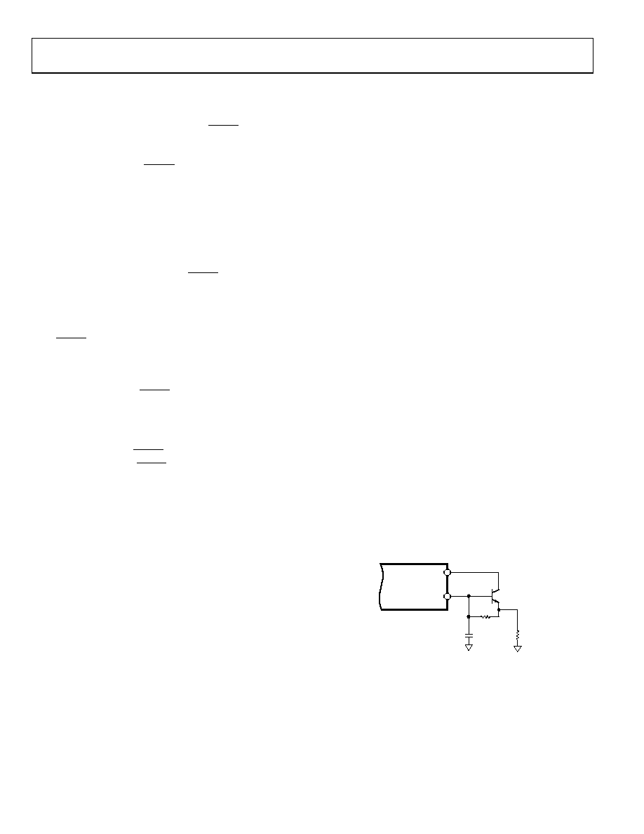
EXTERNAL BOOST FUNCTION
The addition of an external boost transistor, as shown in Figure 41,
reduces the power dissipated in the AD5410/AD5420 by reducing
the current flowing in the on-chip output transistor (dividing it
by the current gain of the external circuit). A discrete NPN
transistor with a breakdown voltage, BVCEO, greater than 40 V
can be used.
used at the extremes of the supply voltage, load current, and
temperature range. The boost transistor can also be used to
reduce the amount of temperature-induced drift in the part.
This minimizes the temperature-induced drift of the on-chip
voltage reference, which improves drift and linearity.
AD5410/
AD5420
MJD31C
OR
2N3053
BOOST
0.022F
RL
1k
IOUT
07027-
036
Figure 41. External Boost Configuration
相关PDF资料 |
PDF描述 |
|---|---|
| UVZ1E682MHD | CAP ALUM 6800UF 25V 20% RADIAL |
| DC245A-A | BOARD EVAL LTC1668 |
| EVAL-AD5570SDZ | BOARD EVAL FOR AD5570 |
| FPF2006 | IC SWITCH LOAD FULL FUNC SC70-5 |
| UCS2G680MNY9 | CAP ALUM 68UF 400V 20% RADIAL |
相关代理商/技术参数 |
参数描述 |
|---|---|
| EVAL-AD5421SDZ | 功能描述:BOARD EVAL FOR AD5421 RoHS:是 类别:编程器,开发系统 >> 评估板 - 数模转换器 (DAC) 系列:- 产品培训模块:Lead (SnPb) Finish for COTS Obsolescence Mitigation Program 标准包装:1 系列:- DAC 的数量:4 位数:12 采样率(每秒):- 数据接口:串行,SPI? 设置时间:3µs DAC 型:电流/电压 工作温度:-40°C ~ 85°C 已供物品:板 已用 IC / 零件:MAX5581 |
| EVAL-AD5422EBZ | 功能描述:BOARD EVAL FOR AD5422 RoHS:是 类别:编程器,开发系统 >> 评估板 - 数模转换器 (DAC) 系列:- 产品培训模块:Lead (SnPb) Finish for COTS Obsolescence Mitigation Program 标准包装:1 系列:- DAC 的数量:4 位数:12 采样率(每秒):- 数据接口:串行,SPI? 设置时间:3µs DAC 型:电流/电压 工作温度:-40°C ~ 85°C 已供物品:板 已用 IC / 零件:MAX5581 |
| EVAL-AD5422LFEBZ | 功能描述:BOARD EVAL FOR AD5422LFEBZ RoHS:否 类别:编程器,开发系统 >> 评估板 - 数模转换器 (DAC) 系列:* 产品培训模块:Lead (SnPb) Finish for COTS Obsolescence Mitigation Program 标准包装:1 系列:- DAC 的数量:4 位数:12 采样率(每秒):- 数据接口:串行,SPI? 设置时间:3µs DAC 型:电流/电压 工作温度:-40°C ~ 85°C 已供物品:板 已用 IC / 零件:MAX5581 |
| EVAL-AD5424EB | 制造商:Analog Devices 功能描述:EVALUATION BOARD I.C. - Bulk 制造商:Rochester Electronics LLC 功能描述: |
| EVAL-AD5424EBZ | 功能描述:BOARD EVALUATION FOR AD5424 RoHS:是 类别:编程器,开发系统 >> 评估板 - 数模转换器 (DAC) 系列:- 产品培训模块:Lead (SnPb) Finish for COTS Obsolescence Mitigation Program 标准包装:1 系列:- DAC 的数量:4 位数:12 采样率(每秒):- 数据接口:串行,SPI? 设置时间:3µs DAC 型:电流/电压 工作温度:-40°C ~ 85°C 已供物品:板 已用 IC / 零件:MAX5581 |
发布紧急采购,3分钟左右您将得到回复。