- 您现在的位置:买卖IC网 > PDF目录17076 > EVAL-AD5424EBZ (Analog Devices Inc)BOARD EVALUATION FOR AD5424 PDF资料下载
参数资料
| 型号: | EVAL-AD5424EBZ |
| 厂商: | Analog Devices Inc |
| 文件页数: | 17/29页 |
| 文件大小: | 0K |
| 描述: | BOARD EVALUATION FOR AD5424 |
| 产品培训模块: | DAC Architectures |
| 标准包装: | 1 |
| DAC 的数量: | 1 |
| 位数: | 8 |
| 采样率(每秒): | 20.4M |
| 数据接口: | 并联 |
| 设置时间: | 30µs |
| DAC 型: | 电流 |
| 工作温度: | -40°C ~ 125°C |
| 已供物品: | 板,CD |
| 已用 IC / 零件: | AD5424 |
| 相关产品: | AD5424YRUZ-REEL7-ND - IC DAC 8BIT MULTIPLYING 16-TSSOP AD5424YRUZ-REEL-ND - IC DAC 8BIT MULTIPLYING 16-TSSOP AD5424YRUZ-ND - IC DAC 8BIT MULTIPLYING 16-TSSOP AD5424YRU-REEL7-ND - IC DAC 8BIT MULTIPLYING 20-TSSOP AD5424YRU-ND - IC DAC 8BIT MULTIPLYING 16-TSSOP AD5424YCPZ-REEL7-ND - IC DAC 8BIT MULTIPLYING 20-LFCSP AD5424YCPZ-ND - IC DAC 8BIT MULTIPLYING 20-LFCSP |
第1页第2页第3页第4页第5页第6页第7页第8页第9页第10页第11页第12页第13页第14页第15页第16页当前第17页第18页第19页第20页第21页第22页第23页第24页第25页第26页第27页第28页第29页
Data Sheet
AD5424/AD5433/AD5445
Rev. D | Page 23 of 28
Provided the DAC switches are driven from true wideband
low impedance sources (VIN and AGND), they settle quickly.
Consequently, the slew rate and settling time of a voltage
switching DAC circuit is determined largely by the output op
amp. To obtain minimum settling time in this configuration, it
is important to minimize capacitance at the VREF node (voltage
output node in this application) of the DAC. This is done by using
low inputs capacitance buffer amplifiers and careful board design.
Most single-supply circuits include ground as part of the analog
signal range, which in turns requires an amplifier that can handle
rail-to-rail signals. There is a large range of single-supply
amplifiers available from Analog Devices.
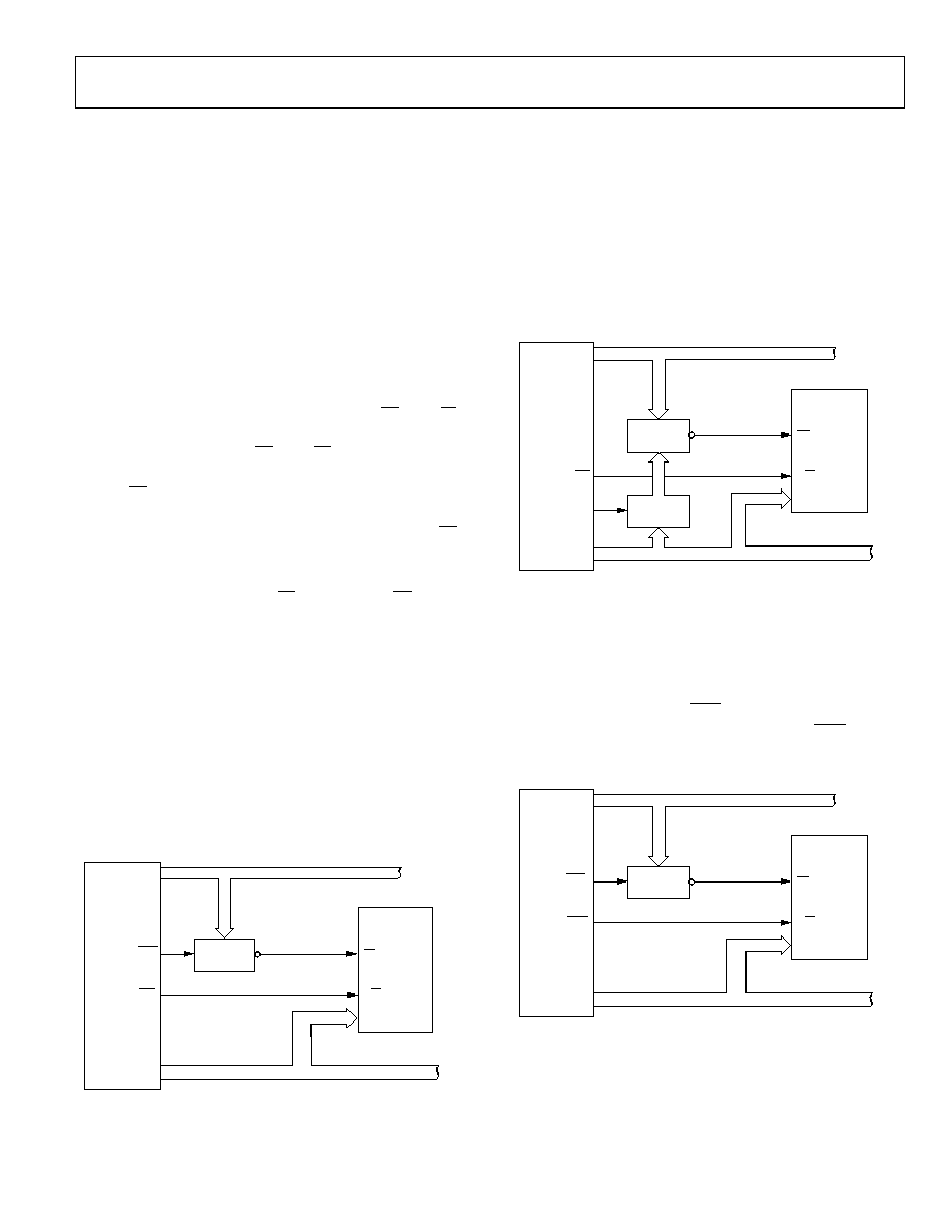
PARALLEL INTERFACE
of an 8-, 10-, or 12-bit parallel word. Control lines CS and R/W
allow data to be written to or read from the DAC register. A
write event takes place when CS and R/W are brought low, data
available on the data lines fills the shift register, and the rising
edge of CS latches the data and transfers the latched data-word
to the DAC register. The DAC latches are not transparent, thus
a write sequence must consist of a falling and rising edge on CS
to ensure that data is loaded to the DAC register and its analog
equivalent is reflected on the DAC output.
A read event takes place when R/W is held high and CS is
brought low. New data is loaded from the DAC register back to
the input register and out onto the data line where it can be read
back to the controller for verification or diagnostic purposes.
MICROPROCESSOR INTERFACING
the ADSP-21xx series of DSPs as a memory-mapped device. A
single wait state may be necessary to interface the AD5424/
speed of the DSP. The wait state can be programmed via the
data memory wait state control register of the ADSP-21xx
(see the ADSP-21xx family user’s manual for details).
03160-056
R/W
DB0 TO DB11
AD5424/
AD5433/
AD5445*
ADDRESS
DECODER
CS
DATA 0 TO
DATA 23
ADDRESS BUS
ADDR0 TO
ADRR13
ADSP-21xx*
DATA BUS
DMS
WR
*ADDITIONAL PINS OMITTED FOR CLARITY
AD5445 and the 8xC51 family of DSPs. To facilitate external
data memory access, the address latch enable (ALE) mode is
enabled. The low byte of the address is latched with this output
pulse during access to external memory. AD0 to AD7 are the
multiplexed low order addresses and data bus and require
strong internal pull-ups when emitting 1s. During access to
external memory, A8 to A15 are the high order address bytes.
Since these ports are open drained, they also require strong
internal pull-ups when emitting 1s.
03160-063
R/W
DB0 TO DB11
AD5424/
AD5433/
AD5445*
ADDRESS
DECODER
CS
AD0 TO AD7
ADDRESS BUS
A8 TO A15
8051*
DATA BUS
WR
*ADDITIONAL PINS OMITTED FOR CLARITY
8-BIT
LATCH
ALE
asynchronous memory write cycle of the processor drives the
digital inputs of the DAC. The AMSx line is actually four memory
select lines. Internal ADDR lines are decoded into AMS3-0, these
lines are then inserted as chip selects. The rest of the interface is
a standard handshaking operation.
03160-057
R/W
DB0 TO DB11
AD5424/
AD5433/
AD5445*
ADDRESS
DECODER
CS
DATA 0 TO
DATA 23
ADDRESS BUS
ADDR1 TO
ADRR19
ADSP-BF5xx
DATA BUS
AMSx
AWE
*ADDITIONAL PINS OMITTED FOR CLARITY
相关PDF资料 |
PDF描述 |
|---|---|
| 0210490943 | CABLE JUMPER 1.25MM .030M 25POS |
| VI-B0K-EY | CONVERTER MOD DC/DC 40V 50W |
| VI-B4D-EY | CONVERTER MOD DC/DC 85V 50W |
| VI-B4B-EY | CONVERTER MOD DC/DC 95V 50W |
| VI-B44-EY | CONVERTER MOD DC/DC 48V 50W |
相关代理商/技术参数 |
参数描述 |
|---|---|
| EVAL-AD5425EB | 制造商:Analog Devices 功能描述:EVALUATION BOARD I.C. - Bulk |
| EVAL-AD5425EBZ | 功能描述:BOARD EVALUATION FOR AD5425 RoHS:是 类别:编程器,开发系统 >> 评估板 - 数模转换器 (DAC) 系列:- 产品培训模块:Lead (SnPb) Finish for COTS Obsolescence Mitigation Program 标准包装:1 系列:- DAC 的数量:4 位数:12 采样率(每秒):- 数据接口:串行,SPI? 设置时间:3µs DAC 型:电流/电压 工作温度:-40°C ~ 85°C 已供物品:板 已用 IC / 零件:MAX5581 |
| EVAL-AD5426EB | 制造商:Analog Devices 功能描述:EVAL BD FOR AD5426, 0BIT HIGH BANDWIDTH MULTIPLYING DACS W/ - Bulk |
| EVAL-AD5428EBZ | 制造商:Analog Devices 功能描述:EVAL BD FOR 8-/10-/12-BIT, PARALLEL INPUT, DUAL-CH, CURRENT - Bulk |
| EVAL-AD5429EB | 制造商:Analog Devices 功能描述:EVALUATION BOARD I.C. - Bulk |
发布紧急采购,3分钟左右您将得到回复。