- 您现在的位置:买卖IC网 > PDF目录17077 > EVAL-AD5443SDZ (Analog Devices Inc)BOARD EVAL FOR AD5443 PDF资料下载
参数资料
| 型号: | EVAL-AD5443SDZ |
| 厂商: | Analog Devices Inc |
| 文件页数: | 9/25页 |
| 文件大小: | 0K |
| 描述: | BOARD EVAL FOR AD5443 |
| 标准包装: | 1 |
| 系列: | * |
AD5426/AD5432/AD5443
Data Sheet
Rev. G | Page 16 of 24
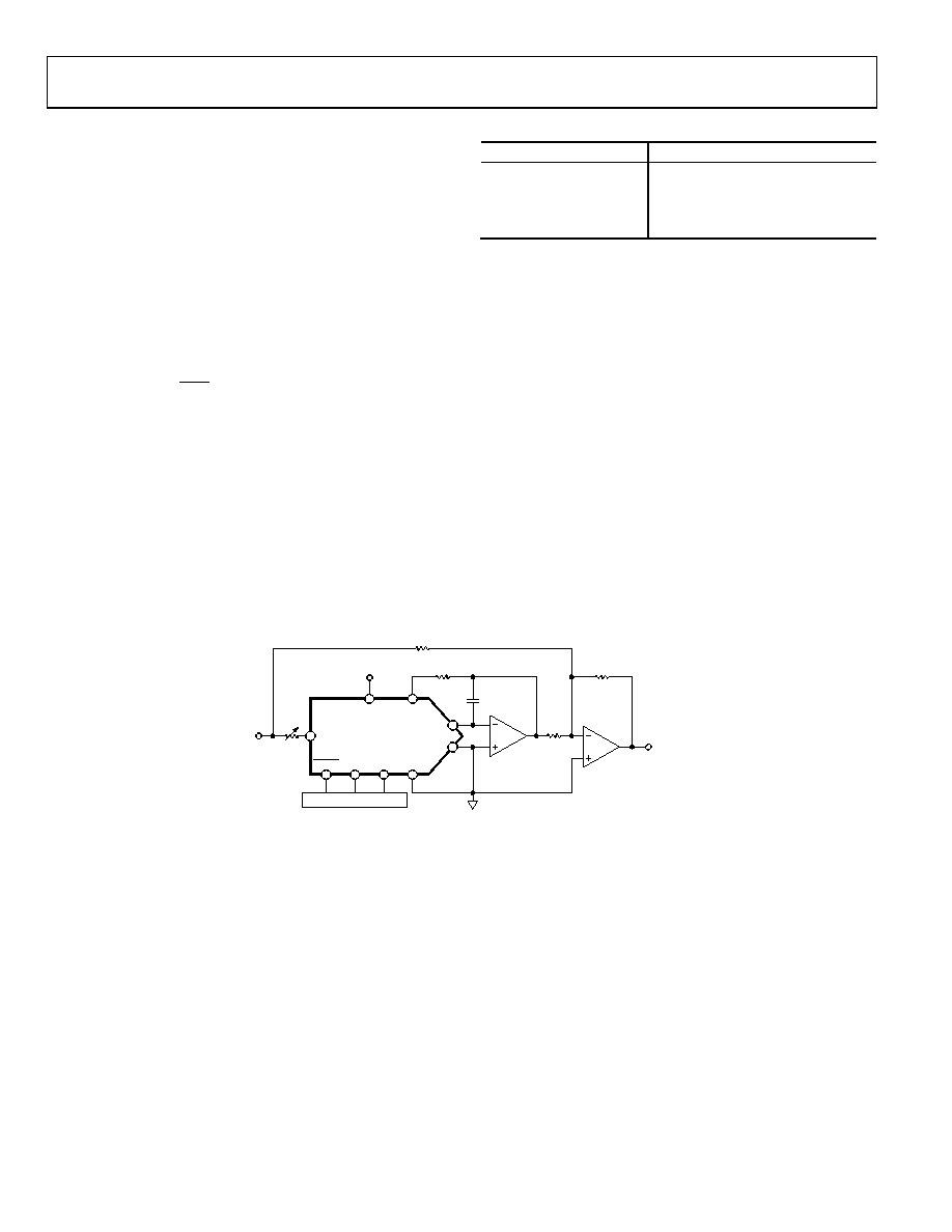
Bipolar Operation
In some applications, it may be necessary to generate full
4-quadrant multiplying operation or a bipolar output swing.
This can easily be accomplished by using another external
amplifier and some external resistors, as shown in Figure 42.
In this circuit, the second amplifier, A2, provides a gain of 2.
Biasing the external amplifier with an offset from the reference
voltage results in full 4-quadrant multiplying operation. The
transfer function of this circuit shows that both negative and
positive output voltages are created as the input data, D, which
is incremented from code zero (VOUT = VREF) to midscale
(VOUT = 0 V) to full scale (VOUT = +VREF).
REF
n
REF
OUT
V
D
V
×
=
1
2
where D is the fractional representation of the digital word
loaded to the DAC and n is the resolution of the DAC.
D = 0 to 255 (8-bit AD5426)
= 0 to 1023 (10-bit AD5432)
= 0 to 4095 (12-bit AD5443)
When VIN is an ac signal, the circuit performs 4-quadrant
multiplication.
Table 6 shows the relationship between digital code and the
expected output voltage for bipolar operation (AD5426,
8-bit device).
Table 6. Bipolar Code Table
Digital Input
Analog Output (V)
1111 1111
+VREF (127/128)
1000 0000
0
0000 0001
VREF (127/128)
0000 0000
VREF (128/128)
Stability
In the I-to-V configuration, the IOUT of the DAC and the inverting
node of the op amp must be connected as close as possible and
proper PCB layout techniques must be employed. Since every
code change corresponds to a step function, gain peaking may
occur if the op amp has limited gain bandwidth product (GBP)
and there is excessive parasitic capacitance at the inverting node.
This parasitic capacitance introduces a pole into the open-loop
response that can cause ringing or instability in closed-loop
applications.
An optional compensation capacitor, C1, can be added in parallel
small a value of C1 can produce ringing at the output, while
too large a value can adversely affect the settling time. C1 should
be found empirically, but 1 pF to 2 pF is generally adequate for
compensation.
VOUT = –VREF
TO +VREF
SCLK SDIN GND
VREF
±10V
SYNC
IOUT2
IOUT1
RFB
AGND
AD5426/
AD5432/
AD5443
R1
R2
A1
VREF
VDD
C1
NOTES
1. R1 AND R2 ARE USED ONLY IF GAIN ADJUSTMENT IS REQUIRED. ADJUST R1 FOR
VOUT = 0V WITH CODE 10000000 LOADED TO DAC.
2. MATCHING AND TRACKING IS ESSENTIAL FOR RESISTOR PAIRS R3 AND R4.
3. C1 PHASE COMPENSATION (1pF TO 2pF) MAY BE REQUIRED IF A1/A2 IS A HIGH
SPEED AMPLIFIER.
MICROCONTROLLER
R4
10k
R5
20k
R3
20k
A2
A1
03162-043
Figure 42. Bipolar Operation
相关PDF资料 |
PDF描述 |
|---|---|
| ESA10DTBD | CONN EDGECARD 20POS R/A .125 SLD |
| UCS2W470MNY9 | CAP ALUM 47UF 450V 20% RADIAL |
| EVAL-AD5445SDZ | BOARD EVAL FOR AD5445 |
| UPZ2G820MNY9 | CAP ALUM 82UF 400V 20% RADIAL |
| V300C2E50BF2 | CONVERTER MOD DC/DC 2V 50W |
相关代理商/技术参数 |
参数描述 |
|---|---|
| EVAL-AD5444EB | 制造商:Analog Devices 功能描述:EVALUATION BOARD I.C. - Bulk |
| EVAL-AD5444EBZ | 制造商:Analog Devices 功能描述:EVAL KIT FOR 12-/14BIT HIGH BANDWIDTH MULTIPLYING DACS W/ SE - Bulk |
| EVAL-AD5445EB | 制造商:Analog Devices 功能描述:EVALUATION BOARD - Bulk |
| EVAL-AD5445EBZ | 功能描述:BOARD EVALUATION FOR AD5445 RoHS:是 类别:编程器,开发系统 >> 评估板 - 数模转换器 (DAC) 系列:- 产品培训模块:Lead (SnPb) Finish for COTS Obsolescence Mitigation Program 标准包装:1 系列:- DAC 的数量:4 位数:12 采样率(每秒):- 数据接口:串行,SPI? 设置时间:3µs DAC 型:电流/电压 工作温度:-40°C ~ 85°C 已供物品:板 已用 IC / 零件:MAX5581 |
| EVAL-AD5445SDZ | 功能描述:BOARD EVAL FOR AD5445 RoHS:是 类别:编程器,开发系统 >> 评估板 - 数模转换器 (DAC) 系列:* 产品培训模块:Lead (SnPb) Finish for COTS Obsolescence Mitigation Program 标准包装:1 系列:- DAC 的数量:4 位数:12 采样率(每秒):- 数据接口:串行,SPI? 设置时间:3µs DAC 型:电流/电压 工作温度:-40°C ~ 85°C 已供物品:板 已用 IC / 零件:MAX5581 |
发布紧急采购,3分钟左右您将得到回复。