- 您现在的位置:买卖IC网 > PDF目录17077 > EVAL-AD5453SDZ (Analog Devices Inc)BOARD EVAL FOR AD5453 PDF资料下载
参数资料
| 型号: | EVAL-AD5453SDZ |
| 厂商: | Analog Devices Inc |
| 文件页数: | 8/28页 |
| 文件大小: | 0K |
| 描述: | BOARD EVAL FOR AD5453 |
| 标准包装: | 1 |
| DAC 的数量: | 1 |
| 位数: | 14 |
| 采样率(每秒): | 2.7M |
| 数据接口: | DSP,MICROWIRE?,QSPI?,串行,SPI? |
| 设置时间: | 180ns |
| DAC 型: | 电流 |
| 工作温度: | -40°C ~ 125°C |
| 已供物品: | 板 |
| 已用 IC / 零件: | AD5453 |
第1页第2页第3页第4页第5页第6页第7页当前第8页第9页第10页第11页第12页第13页第14页第15页第16页第17页第18页第19页第20页第21页第22页第23页第24页第25页第26页第27页第28页
AD5450/AD5451/AD5452/AD5453
Data Sheet
Rev. G | Page 16 of 28
GENERAL DESCRIPTION
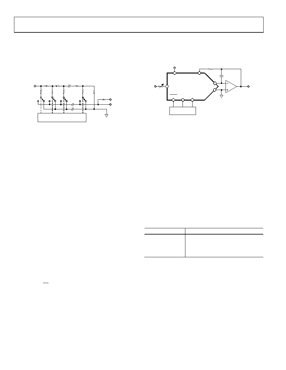
DAC SECTION
current output DACs, respectively, consisting of a segmented
(4-bit) inverting R-2R ladder configuration. A simplified
diagram for the 12-bit AD5452 is shown in Figure 43.
2R
S1
2R
S2
2R
S3
2R
S12
2R
DAC DATA LATCHES
AND DRIVERS
R
RFB
IOUT1
VREF
04587-060
R
AGND
Figure 43. AD5452 Simplified Ladder
The feedback resistor, RFB, has a value of R. The value of R is
typically 9 k (with a minimum value of 7 k and a maximum
value of 11 k). If IOUT1 is kept at the same potential as GND, a
constant current flows in each ladder leg, regardless of digital
input code. Therefore, the input resistance presented at VREF is
always constant and nominally of value R. The DAC output
(IOUT1) is code-dependent, producing various resistances and
capacitances. When choosing the external amplifier, take into
account the variation in impedance generated by the DAC on
the amplifier’s inverting input node.
Access is provided to the VREF, RFB, and IOUT1 terminals of the
DAC, making the device extremely versatile and allowing it to be
configured in several operating modes; for example, it can provide
a unipolar output or can provide 4-quadrant multiplication in
bipolar mode. Note that a matching switch is used in series with
the internal RFB feedback resistor. If users attempt to measure
RFB, power must be applied to VDDto achieve continuity.
CIRCUIT OPERATION
Unipolar Mode
Using a single op amp, these devices can easily be configured to
provide a 2-quadrant multiplying operation or a unipolar output
voltage swing, as shown in Figure 44. When an output amplifier
is connected in unipolar mode, the output voltage is given by
REF
n
OUT
V
D
V
×
=
2
where:
D is the fractional representation of the digital word loaded to
the DAC.
D = 0 to 255 (8-bit AD5450).
= 0 to 1023 (10-bit AD5451).
= 0 to 4095 (12-bit AD5452).
= 0 to 16,383 (14-bit AD5453).
n is the number of bits.
Note that the output voltage polarity is opposite to the VREF
polarity for dc reference voltages.
04587-
009
RFB
IOUT1
GND
SCLK SDIN
VREF
R1
SYNC
AD5450/
AD5451/
AD5452/
AD5453
VDD
AGND
C1
A1
R2
VOUT = 0 TO –VREF
CONTROLLER
NOTES
1. R1 AND R2 USED ONLY IF GAIN ADJUSTMENT IS REQUIRED.
2. C1 PHASE COMPENSATION (1pF TO 2pF) MAY BE REQUIRED
IF A1 IS A HIGH SPEED AMPLIFIER.
Figure 44. Unipolar Mode Operation
These DACs are designed to operate with either negative or
positive reference voltages. The VDD power pin is only used by
the internal digital logic to drive the on and off states of the
DAC switches.
These DACs are designed to accommodate ac reference input
signals in the range of 10 V to +10 V.
With a fixed 10 V reference, the circuit shown in Figure 44 gives
a unipolar 0 V to 10 V output voltage swing. When VIN is an ac
signal, the circuit performs 2-quadrant multiplication.
Table 5 shows the relationship between the digital code and
the expected output voltage for a unipolar operation using the
8-bit AD5450.
Table 5. Unipolar Code Table for the AD5450
Digital Input
Analog Output (V)
1111 1111
VREF (255/256)
1000 0000
VREF (128/256) = VREF/2
0000 0001
VREF (1/256)
0000 0000
VREF (0/256) = 0
相关PDF资料 |
PDF描述 |
|---|---|
| AOZ1360AIL | IC LOAD SW HI-SIDE CC 8SOIC |
| V300C2E50BF | CONVERTER MOD DC/DC 2V 50W |
| EMA10DTBD | CONN EDGECARD 20POS R/A .125 SLD |
| MIC2019A-2YM6 TR | IC POWER SWITCH 2.0A SOT23-6 |
| ECM12DRAN | CONN EDGECARD 24POS R/A .156 SLD |
相关代理商/技术参数 |
参数描述 |
|---|---|
| EVAL-AD5501EBZ | 功能描述:BOARD EVAL FOR AD5501 RoHS:是 类别:编程器,开发系统 >> 评估板 - 数模转换器 (DAC) 系列:- 产品培训模块:Lead (SnPb) Finish for COTS Obsolescence Mitigation Program 标准包装:1 系列:- DAC 的数量:4 位数:12 采样率(每秒):- 数据接口:串行,SPI? 设置时间:3µs DAC 型:电流/电压 工作温度:-40°C ~ 85°C 已供物品:板 已用 IC / 零件:MAX5581 |
| EVAL-AD5504EBZ | 功能描述:BOARD EVAL FOR AD5504 RoHS:是 类别:编程器,开发系统 >> 评估板 - 数模转换器 (DAC) 系列:nanoDAC™ 产品培训模块:Lead (SnPb) Finish for COTS Obsolescence Mitigation Program 标准包装:1 系列:- DAC 的数量:4 位数:12 采样率(每秒):- 数据接口:串行,SPI? 设置时间:3µs DAC 型:电流/电压 工作温度:-40°C ~ 85°C 已供物品:板 已用 IC / 零件:MAX5581 |
| EVAL-AD5516-1EB | 制造商:Analog Devices 功能描述:EVALUATION BOARD I.C. - Bulk |
| EVAL-AD5516-1EBZ | 功能描述:BOARD EVAL FOR AD5516-1 2.5V RoHS:是 类别:编程器,开发系统 >> 评估板 - 数模转换器 (DAC) 系列:- 产品培训模块:Lead (SnPb) Finish for COTS Obsolescence Mitigation Program 标准包装:1 系列:- DAC 的数量:4 位数:12 采样率(每秒):- 数据接口:串行,SPI? 设置时间:3µs DAC 型:电流/电压 工作温度:-40°C ~ 85°C 已供物品:板 已用 IC / 零件:MAX5581 |
| EVAL-AD5516-2EB | 制造商:Analog Devices 功能描述:EVALUATION BOARD I.C. - Bulk |
发布紧急采购,3分钟左右您将得到回复。