- 您现在的位置:买卖IC网 > PDF目录17065 > EVAL-AD5516-2EBZ (Analog Devices Inc)BOARD EVALUATION FOR AD5516-2 PDF资料下载
参数资料
| 型号: | EVAL-AD5516-2EBZ |
| 厂商: | Analog Devices Inc |
| 文件页数: | 2/16页 |
| 文件大小: | 0K |
| 描述: | BOARD EVALUATION FOR AD5516-2 |
| 产品培训模块: | DAC Architectures |
| 标准包装: | 1 |
| DAC 的数量: | 16 |
| 位数: | 14 |
| 采样率(每秒): | 750k |
| 数据接口: | 串行 |
| 设置时间: | 32µs |
| DAC 型: | 电压 |
| 工作温度: | -40°C ~ 85°C |
| 已供物品: | 板 |
| 已用 IC / 零件: | AD5516-2 |
| 相关产品: | AD5516ABCZ-3-ND - IC DAC 12BIT 16CH BIPO 74-CSPBGA AD5516ABCZ-2-ND - IC DAC 12BIT VOUT 16CH 74-CSPBGA AD5516ABC-3-ND - IC DAC 12BIT 16CH 74-CSPBGA AD5516ABC-2-ND - IC DAC 12BIT 16CH 74-CSPBGA AD5516ABC-1-ND - IC DAC 12BIT 16CH 74-CSPBGA |
REV. B
–10–
AD5516
00
A3
A2
A1
A0
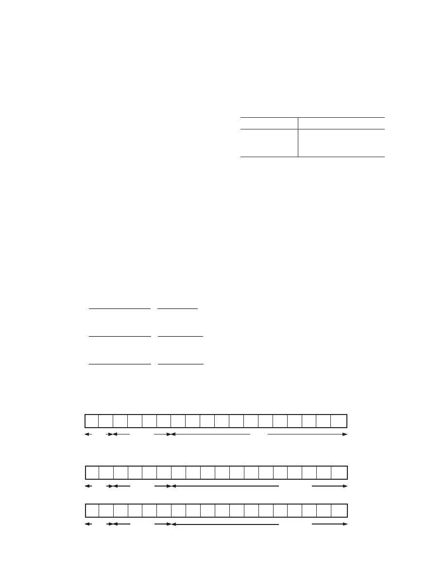
DB11 DB10
DB9
DB8
DB7
DB6
DB5
DB4
DB3
DB2
DB1
DB0
MSB
LSB
MODE
BITS
ADDRESS
BITS
DATA
BITS
Figure 4. Mode 1 Data Format
01
A3
A2
A1
A0
DB11 DB10
DB9
DB8
DB7
DB6
DB5
DB4
DB3
DB2
DB1
DB0
MSB
LSB
MODE
BITS
ADDRESS
BITS
12 INCREMENT
BITS
10
A3
A2
A1
A0
DB11 DB10
DB9
DB8
DB7
DB6
DB5
DB4
DB3
DB2
DB1
DB0
MSB
LSB
MODE
BITS
ADDRESS
BITS
12 DECREMENT
BITS
Figure 5. Mode 2 Data Format
FUNCTIONAL DESCRIPTION
The AD5516 consists of sixteen 12-bit DACs in a single pack-
age. A single reference input pin (REF_IN) is used to provide a
3V reference for all 16 DACs. To update a DAC’s output
voltage, the required DAC is addressed via the 3-wire serial
interface. Once the serial write is complete, the selected DAC
converts the code into an output voltage. The output amplifiers
translate the DAC output range to give the appropriate voltage
range (
±2.5 V, ±5 V, or ±10 V) at output pins VOUT0 to VOUT15.
The AD5516 uses a self-calibrating architecture to achieve 12-bit
performance. The calibration routine servos to select the appro-
priate voltage level on an internal 14-bit resolution DAC.
BUSY
output goes low for the duration of the calibration and further
writes to the AD5516 are ignored while
BUSY is low. BUSY low
time is typically 25
ms. Noise during the calibration (BUSY
low period) can result in the selection of a voltage within a
±0.25 LSB band around the normal selected voltage. See TPC 10.
It is essential to minimize noise on REFIN for optimal perfor-
mance. The AD780’s specified decoupling makes it the ideal
reference to drive the AD5516.
Upon power-on, all DACs power up to a reset value (see the
RESET section).
DIGITAL-TO-ANALOG SECTION
The architecture of each DAC channel consists of a resistor
string DAC followed by an output buffer amplifier with offset
and gain. The voltage at the REF_IN pin provides the reference
voltage for all 16 DACs. The input coding to the DACs is offset
binary; this results in ideal output voltages as follows:
AD5516-1:
V
VD
V
OUT
REF IN
N
REF IN
=
22 5
32
25
3
__
.
–
.
AD5516-2:
V
VD
V
OUT
REF IN
N
REF IN
=
42 5
32
22 5
3
__
.
–
.
AD5516-3:
V
VD
V
OUT
REF IN
N
REF IN
=
82 5
32
42 5
3
__
.
–
.
Where:
D = decimal equivalent of the binary code that is loaded to
the DAC register, i.e., 0–4095
N = DAC resolution = 12
Table I illustrates ideal analog output versus DAC code.
Table I. DAC Register Contents AD5516-1
MSB
LSB
Analog Output, VOUT
1111 1111 1111
VREF_IN
2.5/3 – 1 LSB
1000 0000 0000
0 V
0000 0000 0000
–VREF_IN
2.5/3
MODES OF OPERATION
The AD5516 has two modes of operation.
Mode 1 (MODE bits = 00): The user programs a 12-bit data-
word to one of 16 channels via the serial interface. This word is
loaded into the addressed DAC register and is then converted
into an analog output voltage. During conversion, the
BUSY
output is low and all SCLK pulses are ignored. At the end of a
conversion
BUSY goes high, indicating that the update of the
addressed DAC is complete. It is recommended that SCLK is not
pulsed while
BUSY is low. Mode 1 conversion takes 25
ms typ.
Mode 2 (MODE bits = 01 or 10): Mode 2 operation allows the
user to increment or decrement the DAC output in 0.25 LSB steps,
resulting in a 14-bit monotonic DAC. The amount by which the
DAC output is incremented or decremented is determined by
Mode 2 bits DB11–DB0, e.g., for a 0.25 LSB increment/decrement
DB11...DB0 = 0000 0000 0001, while for a 2.5 LSB increment/
decrement, DB11...DB0 = 0000 0000 1010. The MODE bits
determine whether the DAC data is incremented (01) or dec-
remented (10). The maximum amount that the user is allowed
to increment or decrement the DAC output is 4095 steps of
0.25 LSB, i.e., DB11...DB0 = 1111 1111 1111. Mode 2 update
takes approximately 1
ms. The Mode 2 feature allows increased
resolution, but overall increment/decrement accuracy varies with
increment/decrement step as shown in TPC 14 and TPC 15.
Mode 2 is useful in applications where greater resolution is
required, for example, in servo applications requiring fine-tune
to 14-bit resolution.
相关PDF资料 |
PDF描述 |
|---|---|
| EVAL-AD5516-3EBZ | BOARD EVALUATION AD5516 |
| LLS2E331MELA | CAP ALUM 330UF 250V 20% SNAP |
| SLP561M180C3P3 | CAP ALUM 560UF 180V 20% SNAP |
| SDR0403-2R2ML | INDUCTOR POWER 2.2UH 2.6A 0403 |
| EVAL-AD5570EBZ | BOARD EVALUATION FOR AD5570 |
相关代理商/技术参数 |
参数描述 |
|---|---|
| EVAL-AD5516-3EB | 制造商:AD 制造商全称:Analog Devices 功能描述:16-Channel, 12-Bit Voltage-Output DAC with 14-Bit Increment Mode |
| EVAL-AD5516-3EBZ | 功能描述:BOARD EVALUATION AD5516 RoHS:是 类别:编程器,开发系统 >> 评估板 - 数模转换器 (DAC) 系列:- 产品培训模块:Lead (SnPb) Finish for COTS Obsolescence Mitigation Program 标准包装:1 系列:- DAC 的数量:4 位数:12 采样率(每秒):- 数据接口:串行,SPI? 设置时间:3µs DAC 型:电流/电压 工作温度:-40°C ~ 85°C 已供物品:板 已用 IC / 零件:MAX5581 |
| EVAL-AD5520EB | 制造商:AD 制造商全称:Analog Devices 功能描述:Per Pin Parametric Measurement Unit/Source Measure Unit |
| EVAL-AD5520EBZ | 功能描述:BOARD EVAL FOR AD5520 RoHS:是 类别:编程器,开发系统 >> 评估演示板和套件 系列:- 标准包装:1 系列:PSoC® 主要目的:电源管理,热管理 嵌入式:- 已用 IC / 零件:- 主要属性:- 次要属性:- 已供物品:板,CD,电源 |
| EVAL-AD5522EBDZ | 功能描述:BOARD EVAL FOR 14X14MM AD5522 RoHS:是 类别:编程器,开发系统 >> 评估演示板和套件 系列:- 标准包装:1 系列:PSoC® 主要目的:电源管理,热管理 嵌入式:- 已用 IC / 零件:- 主要属性:- 次要属性:- 已供物品:板,CD,电源 |
发布紧急采购,3分钟左右您将得到回复。