- 您现在的位置:买卖IC网 > PDF目录17080 > EVAL-AD5546SDZ (Analog Devices Inc)BOARD EVAL FOR AD5546 PDF资料下载
参数资料
| 型号: | EVAL-AD5546SDZ |
| 厂商: | Analog Devices Inc |
| 文件页数: | 7/20页 |
| 文件大小: | 0K |
| 描述: | BOARD EVAL FOR AD5546 |
| 标准包装: | 1 |
| 系列: | * |
Data Sheet
AD5546/AD5556
Rev. D | Page 15 of 20
REFERENCE SELECTION
When selecting a reference for use with the AD55xx series
of current output DACs, pay attention to the output voltage
temperature coefficient specification of the reference. Choosing
a precision reference with a low output temperature coefficient
minimizes error sources. Table 11 lists some of the references
available from Analog Devices that are suitable for use with this
range of current output DACs.
AMPLIFIER SELECTION
The primary requirement for the current-steering mode is an
amplifier with low input bias currents and low input offset voltage.
Because of the code-dependent output resistance of the DAC,
the input offset voltage of an op amp is multiplied by the variable
gain of the circuit. A change in this noise gain between two
adjacent digital fractions produces a step change in the output
voltage due to the amplifier’s input offset voltage. This output
voltage change is superimposed on the desired change in output
between the two codes and gives rise to a differential linearity
error, which, if large enough, can cause the DAC to be
nonmonotonic.
The input bias current of an op amp also generates an offset at
the voltage output because of the bias current flowing in the
feedback resistor, RFB.
Common-mode rejection of the op amp is important in voltage-
switching circuits because it produces a code-dependent error
at the voltage output of the circuit.
Provided that the DAC switches are driven from true wideband
low impedance sources, they settle quickly. Consequently, the
slew rate and settling time of a voltage-switching DAC circuit is
determined largely by the output op amp. To obtain minimum
settling time in this configuration, minimize capacitance at the
VREF node (the voltage output node in this application) of the
DAC. This is done by using low input capacitance buffer
amplifiers and careful board design.
Analog Devices offers a wide range of amplifiers for both precision
dc and ac applications, as listed in Table 12 and Table 13.
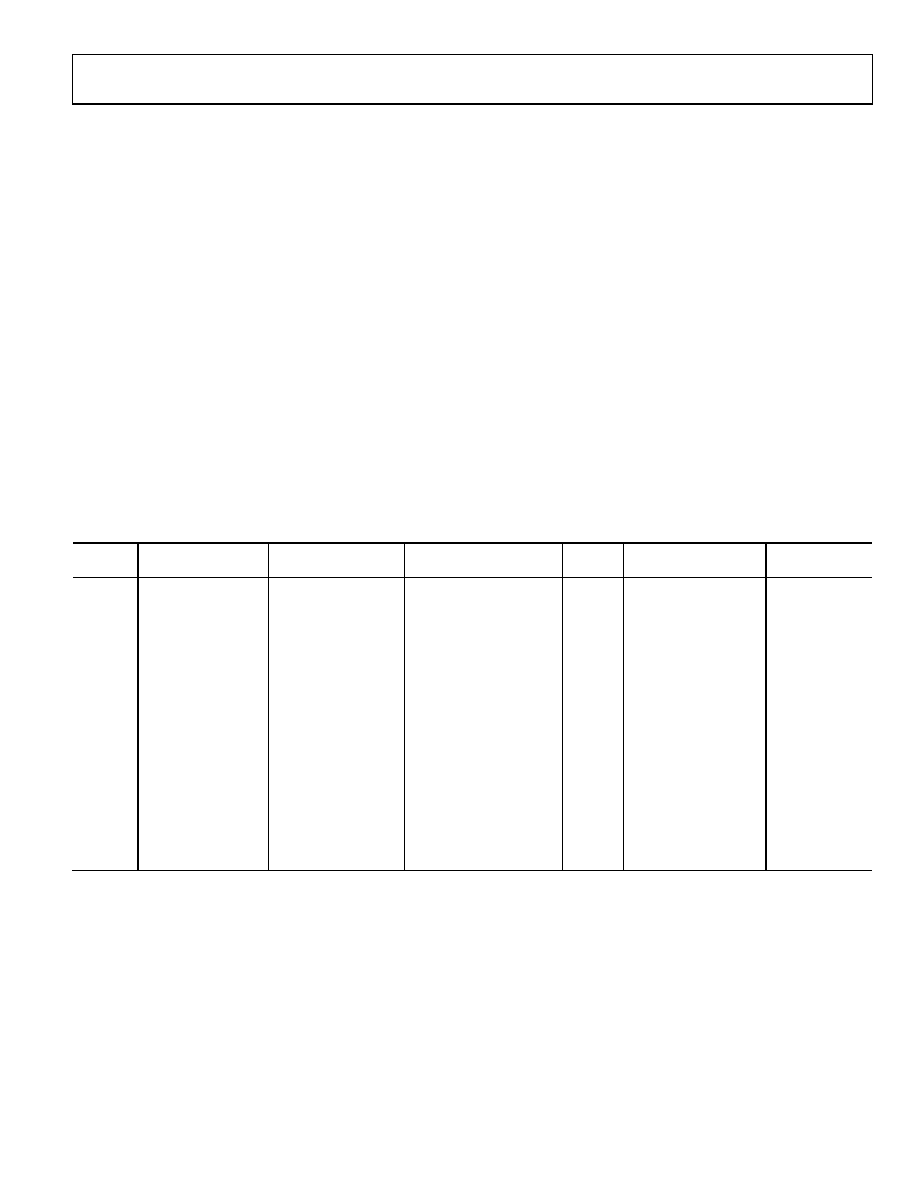
Table 11. Suitable Analog Devices Precision References
Part No.
Output Voltage (V)
Initial Tolerance (%)
Maximum Temperature
Drift (ppm/°C)
ISS (mA)
Output Noise (V p-p)
Package(s)
10
0.05
3
1
20
SOIC-8
10
0.05
9
1
20
TSOT-5, SC70-5
5.0
0.06
3
1
10
SOIC-8
5.0
0.06
9
1
10
TSOT-5, SC70-5
2.5
0.1
3
1
6
SOIC-8
2.5
0.1
9
1
6
TSOT-5, SC70-5
3.0
0.1
3
1
10
SOIC-8
3.0
0.1
9
1
10
TSOT-5, SC70-5
2.048
0.05
3
0.5
1.75
SOIC-8, MSOP-8
2.50
0.04
3
0.5
1.75
SOIC-8, MSOP-8
3.00
0.04
3
0.5
2
SOIC-8, MSOP-8
5.00
0.04
3
0.5
3.4
SOIC-8, MSOP-8
2.500
0.04
3
0.8
3.5
SOIC-8, MSOP-8
5.000
0.04
3
0.8
8
SOIC-8, MSOP-8
2.5
0.16
9
0.12
5
TSOT-5
5.0
0.10
9
0.12
8
TSOT-5
相关PDF资料 |
PDF描述 |
|---|---|
| V48C2E50BL | CONVERTER MOD DC/DC 2V 50W |
| AP2152AFGEG-7 | IC PWR SW USB 2CH 0.5A 8-DFN |
| 0210390971 | CABLE JUMPER 1MM .102M 27POS |
| AIMC-0402-R12J-T | INDUCTOR MULTILAYER 120NH 0402 |
| RCC22DCSD | CONN EDGECARD 44POS DIP .100 SLD |
相关代理商/技术参数 |
参数描述 |
|---|---|
| EVAL-AD5551/52EB | 制造商:Analog Devices 功能描述:EVAL KIT FOR AD5551 5 V, SERL-INPUT VOLT-OUTPUT, 14BIT DACS - Bulk |
| EVAL-AD5560EBUZ | 功能描述:BOARD EVALUATION FOR AD5560 RoHS:是 类别:编程器,开发系统 >> 评估演示板和套件 系列:- 标准包装:1 系列:PSoC® 主要目的:电源管理,热管理 嵌入式:- 已用 IC / 零件:- 主要属性:- 次要属性:- 已供物品:板,CD,电源 |
| EVAL-AD5570EB | 制造商:Analog Devices 功能描述:DEV TOOLS, TRUE ACCURACY, 16BIT 12V/ 15V, SERL INPUT VOLT O - Bulk |
| EVAL-AD5570EBZ | 功能描述:BOARD EVALUATION FOR AD5570 RoHS:是 类别:编程器,开发系统 >> 评估板 - 数模转换器 (DAC) 系列:- 产品培训模块:Lead (SnPb) Finish for COTS Obsolescence Mitigation Program 标准包装:1 系列:- DAC 的数量:4 位数:12 采样率(每秒):- 数据接口:串行,SPI? 设置时间:3µs DAC 型:电流/电压 工作温度:-40°C ~ 85°C 已供物品:板 已用 IC / 零件:MAX5581 |
| EVAL-AD5570SDZ | 功能描述:BOARD EVAL FOR AD5570 RoHS:是 类别:编程器,开发系统 >> 评估板 - 数模转换器 (DAC) 系列:- 产品培训模块:Lead (SnPb) Finish for COTS Obsolescence Mitigation Program 标准包装:1 系列:- DAC 的数量:4 位数:12 采样率(每秒):- 数据接口:串行,SPI? 设置时间:3µs DAC 型:电流/电压 工作温度:-40°C ~ 85°C 已供物品:板 已用 IC / 零件:MAX5581 |
发布紧急采购,3分钟左右您将得到回复。