- 您现在的位置:买卖IC网 > PDF目录17070 > EVAL-AD5680EBZ (Analog Devices Inc)BOARD EVAL FOR AD5680 PDF资料下载
参数资料
| 型号: | EVAL-AD5680EBZ |
| 厂商: | Analog Devices Inc |
| 文件页数: | 8/20页 |
| 文件大小: | 0K |
| 描述: | BOARD EVAL FOR AD5680 |
| 产品培训模块: | DAC Architectures |
| 标准包装: | 1 |
| 系列: | nanoDAC™ |
| DAC 的数量: | 1 |
| 位数: | 18 |
| 采样率(每秒): | 12.5k |
| 数据接口: | 串行 |
| 设置时间: | 80µs |
| DAC 型: | 电压 |
| 工作温度: | -40°C ~ 105°C |
| 已供物品: | 板 |
| 已用 IC / 零件: | AD5680 |
| 相关产品: | AD5680BRJZ-1500RL7DKR-ND - IC DAC 18BIT 5V SOT23-8 AD5680BRJZ-1500RL7CT-ND - IC DAC 18BIT 5V SOT23-8 AD5680BRJZ-2REEL7DKR-ND - IC DAC 18BIT 5V SOT23-8 AD5680BRJZ-2REEL7CT-ND - IC DAC 18BIT 5V SOT23-8 AD5680BRJZ-2REEL7TR-ND - IC DAC 18BIT 5V SOT23-8 AD5680BRJZ-2500RL7TR-ND - IC DAC 18BIT 5V SOT23-8 AD5680BRJZ-1500RL7TR-ND - IC DAC 18BIT 5V SOT23-8 |
AD5680
Data Sheet
USING A REFERENCE AS A POWER SUPPLY FOR
Because the supply current required by the AD5680 is extremely
low, an alternative option is to use a voltage reference to supply
the required voltage to the part (see Figure 36). This is especially
useful if the power supply is quite noisy, or if the system supply
voltages are at some value other than 5 V, for example, 15 V.
The voltage reference outputs a steady supply voltage for the
AD5680; see Table 6 for a suitable reference. If the low dropout
with no load on the output of the DAC. When the DAC output
is loaded, the REF195 also needs to supply the current to the
load. The total current required (with a 5 k load on the DAC
output) is
325 A + (5 V/5 k) = 1.33 mA
The load regulation of the REF195 is typically 2 ppm/mA,
which results in a 2.7 ppm (13.5 V) error for the 1.33 mA
current drawn from it. This corresponds to a 0.177 LSB error.
AD5680
SYNC
SCLK
DIN
15V
5V
VOUT = 0V TO 5V
VREF
VDD
REF195
05854-
040
250A
3-WIRE
SERIAL
INTERFACE
Figure 36. REF195 as Power Supply to the AD5680
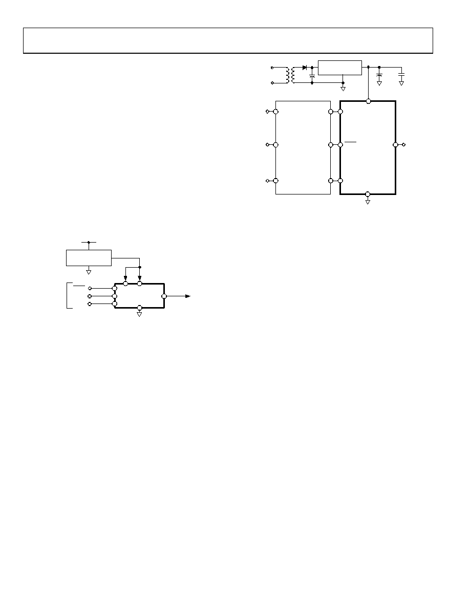
USING THE AD5680 WITH A GALVANICALLY
ISOLATED INTERFACE
In process-control applications in industrial environments, it is
often necessary to use a galvanically isolated interface to protect
and isolate the controlling circuitry from any hazardous common-
mode voltages that might occur in the area where the DAC is
functioning. Isocouplers provide isolation in excess of 3 kV. The
AD5680 uses a 3-wire serial logic interface, so the ADuM130x
3-channel digital isolator provides the required isolation (see
Figure 37). The power supply to the part also needs to be isolated,
which is done by using a transformer. On the DAC side of the
transformer, a 5 V regulator provides the 5 V supply required
for the AD5680.
0.1F
5V
REGULATOR
GND
05854-
041
DIN
SYNC
SCLK
POWER
10F
SDI
SCLK
DATA
AD5680
VOUT
VOB
VOA
VOC
VDD
VIC
VIB
VIA
ADuM130x
Figure 37. AD5680 with a Galvanically Isolated Interface
POWER SUPPLY BYPASSING AND GROUNDING
When accuracy is important in a circuit, it is helpful to carefully
consider the power supply and ground return layout on the board.
The printed circuit board containing the AD5680 should have
separate analog and digital sections, each having its own area of
the board. If the AD5680 is in a system where other devices
require an AGND-to-DGND connection, the connection should
be made at one point only. This ground point should be as close
as possible to the AD5680.
The power supply to the AD5680 should be bypassed with 10 F
and 0.1 F capacitors. The capacitors should be located as close
as possible to the device, with the 0.1 F capacitor ideally right
up against the device. The 10 F capacitors should be the tanta-
lum bead type. It is important that the 0.1 F capacitor has low
effective series resistance (ESR) and effective series inductance
(ESI), for example, common ceramic types of capacitors. This
0.1 F capacitor provides a low impedance path to ground for
high frequencies caused by transient currents due to internal
logic switching.
The power supply line itself should have as large a trace as
possible to provide a low impedance path and to reduce glitch
effects on the supply line. Clocks and other fast switching digital
signals should be shielded from other parts of the board by
digital ground. Avoid crossover of digital and analog signals if
possible. When traces cross on opposite sides of the board,
ensure that they run at right angles to each other to reduce
feedthrough effects on the board. The best board layout tech-
nique is the microstrip technique where the component side of
the board is dedicated to the ground plane only and the signal
traces are placed on the solder side. However, this is not always
possible with a 2-layer board.
Rev. B | Page 16 of 20
相关PDF资料 |
PDF描述 |
|---|---|
| NRS6010T1R5MMGF | INDUCTOR POWER 1.5UH 1.9A SMD |
| 0210490965 | CABLE JUMPER 1.25MM .030M 27POS |
| NR6045T680M | INDUCTOR 68UH 900MA 20% SMD |
| SRN6045-470M | INDUCTOR POWER SHIELD 47UH SMD |
| MIC2026-2YM TR | IC SW DISTRIBUTION 2CHAN 8SOIC |
相关代理商/技术参数 |
参数描述 |
|---|---|
| EVAL-AD5684RSDZ | 功能描述:BOARD EVAL FOR AD5684R RoHS:是 类别:编程器,开发系统 >> 评估板 - 数模转换器 (DAC) 系列:nanoDAC™ 产品培训模块:Lead (SnPb) Finish for COTS Obsolescence Mitigation Program 标准包装:1 系列:- DAC 的数量:4 位数:12 采样率(每秒):- 数据接口:串行,SPI? 设置时间:3µs DAC 型:电流/电压 工作温度:-40°C ~ 85°C 已供物品:板 已用 IC / 零件:MAX5581 |
| EVAL-AD5686RSDZ | 功能描述:BOARD EVAL FOR AD5686R RoHS:是 类别:编程器,开发系统 >> 评估板 - 数模转换器 (DAC) 系列:nanoDAC™ 产品培训模块:Lead (SnPb) Finish for COTS Obsolescence Mitigation Program 标准包装:1 系列:- DAC 的数量:4 位数:12 采样率(每秒):- 数据接口:串行,SPI? 设置时间:3µs DAC 型:电流/电压 工作温度:-40°C ~ 85°C 已供物品:板 已用 IC / 零件:MAX5581 |
| EVAL-AD5687RSDZ | 功能描述:数据转换 IC 开发工具 RoHS:否 制造商:Texas Instruments 产品:Demonstration Kits 类型:ADC 工具用于评估:ADS130E08 接口类型:SPI 工作电源电压:- 6 V to + 6 V |
| EVAL-AD5689RSDZ | 功能描述:数据转换 IC 开发工具 EVALUATION BOARD RoHS:否 制造商:Texas Instruments 产品:Demonstration Kits 类型:ADC 工具用于评估:ADS130E08 接口类型:SPI 工作电源电压:- 6 V to + 6 V |
| EVAL-AD5694RSDZ | 功能描述:BOARD EVAL FOR AD5694R RoHS:是 类别:编程器,开发系统 >> 评估板 - 数模转换器 (DAC) 系列:nanoDAC™ 产品培训模块:Lead (SnPb) Finish for COTS Obsolescence Mitigation Program 标准包装:1 系列:- DAC 的数量:4 位数:12 采样率(每秒):- 数据接口:串行,SPI? 设置时间:3µs DAC 型:电流/电压 工作温度:-40°C ~ 85°C 已供物品:板 已用 IC / 零件:MAX5581 |
发布紧急采购,3分钟左右您将得到回复。