- 您现在的位置:买卖IC网 > PDF目录17066 > EVAL-AD5764REBZ (Analog Devices Inc)EVAL BOARD FOR AD5764 PDF资料下载
参数资料
| 型号: | EVAL-AD5764REBZ |
| 厂商: | Analog Devices Inc |
| 文件页数: | 14/32页 |
| 文件大小: | 0K |
| 描述: | EVAL BOARD FOR AD5764 |
| 标准包装: | 1 |
| DAC 的数量: | 4 |
| 位数: | 16 |
| 数据接口: | DSP,MICROWIRE?,QSPI?,串行,SPI? |
| 设置时间: | 8µs |
| DAC 型: | 电压 |
| 工作温度: | -40°C ~ 85°C |
| 已供物品: | 板,CD |
| 已用 IC / 零件: | AD5764R |
第1页第2页第3页第4页第5页第6页第7页第8页第9页第10页第11页第12页第13页当前第14页第15页第16页第17页第18页第19页第20页第21页第22页第23页第24页第25页第26页第27页第28页第29页第30页第31页第32页
Data Sheet
AD5764R
Rev. D | Page 21 of 32
THEORY OF OPERATION
The AD5764R is a quad, 16-bit, serial input, bipolar voltage output
DAC that operates from supply voltages of ±11.4 V to ±16.5 V and
has a buffered output voltage of up to ±10.5263 V. Data is written to
the AD5764R in a 24-bit word format via a 3-wire serial interface.
The AD5764R also offers an SDO pin that is available for daisy
chaining or readback.
The AD5764R incorporates a power-on reset circuit that ensures
that the data registers are loaded with 0x0000 at power-up. The
AD5764R features a digital I/O port that can be programmed via
the serial interface, an analog die temperature sensor, on-chip
10 ppm/°C voltage reference, on-chip reference buffers, and per
channel digital gain and offset registers.
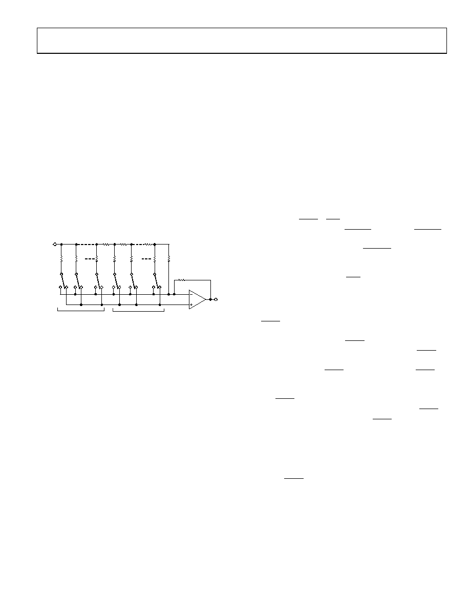
DAC ARCHITECTURE
The DAC architecture of the AD5764R consists of a 16-bit,
current mode, segmented R-2R DAC. The simplified circuit
diagram for the DAC section is shown in Figure 39.
06064-
060
2R
E15
VREF
2R
E14
E1
2R
S11
R
2R
S10
2R
12-BIT, R-2R LADDER
4 MSBs DECODED INTO
15 EQUAL SEGMENTS
VOUTx
2R
S0
2R
AGNDx
R/8
IOUT
Figure 39. DAC Ladder Structure
The four MSBs of the 16-bit data-word are decoded to drive
15 switches, E1 to E15. Each of these switches connects one
of the 15 matched resistors to either AGNDx or IOUT. The
remaining 12 bits of the data-word drive Switch S0 to Switch S11
of the 12-bit R-2R ladder network.
REFERENCE BUFFERS
The AD5764R can operate with either an external or an internal
reference. The reference inputs (REFAB and REFCD) have an
input range of up to 7 V. This input voltage is then used to provide
a buffered positive and negative reference for the DAC cores.
The positive reference is given by
+VREF = 2 × VREFIN
The negative reference to the DAC cores is given by
VREF = 2 × VREFIN
These positive and negative reference voltages (along with the
gain register values) define the output ranges of the DACs.
SERIAL INTERFACE
The AD5764R is controlled over a versatile 3-wire serial interface
that operates at clock rates of up to 30 MHz and is compatible
with SPI, QSPI, MICROWIRE, and DSP standards.
Input Shift Register
The input shift register is 24 bits wide. Data is loaded into the
device, MSB first, as a 24-bit word under the control of a serial
clock input, SCLK. The input register consists of a read/write bit,
a reserved bit that must be set to 0, three register select bits, three
DAC address bits, and 16 data bits, as shown in Table 9. The
timing diagram for this operation is shown in Figure 2.
Upon power-up, the data registers are loaded with zero code
(0x0000) and the outputs are clamped to 0 V via a low impedance
path. The outputs can be updated with the zero code value by
asserting either LDAC or CLR. The corresponding output voltage
depends on the state of the BIN/2sCOMP pin. If the BIN/2sCOMP
pin is tied to DGND, the data coding is twos complement and
the outputs update to 0 V. If the BIN/2sCOMP pin is tied to
DVCC, the data coding is offset binary and the outputs update to
negative full scale. To have the outputs power up with zero code
loaded to the outputs, hold the CLR pin low during power-up.
Standalone Operation
The serial interface works with both a continuous and noncon-
tinuous serial clock. A continuous SCLK source can be used only
if SYNC is held low for the correct number of clock cycles. In
gated clock mode, a burst clock containing the exact number of
clock cycles must be used, and SYNC must be taken high after
the final clock to latch the data. The first falling edge of SYNC
starts the write cycle. Exactly 24 falling clock edges must be
applied to SCLK before SYNC is brought high again. If SYNC is
brought high before the 24th falling SCLK edge, then the data
written is invalid. If more than 24 falling SCLK edges are applied
before SYNC is brought high, the input data is also invalid. The
input register addressed is updated on the rising edge of SYNC.
For another serial transfer to take place, SYNC must be brought
low again. After the end of the serial data transfer, data is
automatically transferred from the input shift register to the
addressed register.
When the data has been transferred into the chosen register of
the addressed DAC, all data registers and outputs can be updated
by taking LDAC low.
相关PDF资料 |
PDF描述 |
|---|---|
| RBA10DTAI | CONN EDGECARD 20POS R/A .125 SLD |
| GBM28DRUI | CONN EDGECARD 56POS DIP .156 SLD |
| 0210390934 | CABLE JUMPER 1MM .203M 23POS |
| AP2182SG-13 | IC PWR SW USB 2CH 1.5A 8-SOIC |
| GCM11DRYF | CONN EDGECARD 22POS DIP .156 SLD |
相关代理商/技术参数 |
参数描述 |
|---|---|
| EVAL-AD5765EBZ | 功能描述:BOARD EVAL FOR AD5765 RoHS:是 类别:编程器,开发系统 >> 评估板 - 数模转换器 (DAC) 系列:* 产品培训模块:Lead (SnPb) Finish for COTS Obsolescence Mitigation Program 标准包装:1 系列:- DAC 的数量:4 位数:12 采样率(每秒):- 数据接口:串行,SPI? 设置时间:3µs DAC 型:电流/电压 工作温度:-40°C ~ 85°C 已供物品:板 已用 IC / 零件:MAX5581 |
| EVAL-AD5780SDZ | 功能描述:BOARD EVALUATION FOR AD5780 RoHS:是 类别:编程器,开发系统 >> 评估板 - 数模转换器 (DAC) 系列:- 产品培训模块:Lead (SnPb) Finish for COTS Obsolescence Mitigation Program 标准包装:1 系列:- DAC 的数量:4 位数:12 采样率(每秒):- 数据接口:串行,SPI? 设置时间:3µs DAC 型:电流/电压 工作温度:-40°C ~ 85°C 已供物品:板 已用 IC / 零件:MAX5581 |
| EVAL-AD5781SDZ | 功能描述:BOARD EVAL FOR AD5781 RoHS:是 类别:编程器,开发系统 >> 评估板 - 数模转换器 (DAC) 系列:- 产品培训模块:Lead (SnPb) Finish for COTS Obsolescence Mitigation Program 标准包装:1 系列:- DAC 的数量:4 位数:12 采样率(每秒):- 数据接口:串行,SPI? 设置时间:3µs DAC 型:电流/电压 工作温度:-40°C ~ 85°C 已供物品:板 已用 IC / 零件:MAX5581 |
| EVAL-AD5790SDZ | 制造商:Analog Devices 功能描述:AD5790 DAC EVALUATION BOARD 制造商:Analog Devices 功能描述:AD5790, DAC, EVALUATION BOARD 制造商:Analog Devices 功能描述:AD5790, DAC, EVALUATION BOARD, Silicon Manufacturer:Analog Devices, Silicon Core 制造商:Analog Devices 功能描述:AD5790, DAC, EVALUATION BOARD, Silicon Manufacturer:Analog Devices, Silicon Core Number:(Not Applicable), Kit Application Type:(Not Available), Application Sub Type:DAC, Features:20-bit Voltage Output DAC, Integrated Precision , RoHS Compliant: Yes |
| EVAL-AD5791SDZ | 功能描述:BOARD EVAL FOR AD5791 RoHS:是 类别:编程器,开发系统 >> 评估板 - 数模转换器 (DAC) 系列:- 产品培训模块:Lead (SnPb) Finish for COTS Obsolescence Mitigation Program 标准包装:1 系列:- DAC 的数量:4 位数:12 采样率(每秒):- 数据接口:串行,SPI? 设置时间:3µs DAC 型:电流/电压 工作温度:-40°C ~ 85°C 已供物品:板 已用 IC / 零件:MAX5581 |
发布紧急采购,3分钟左右您将得到回复。