- 您现在的位置:买卖IC网 > PDF目录17103 > EVAL-AD5791SDZ (Analog Devices Inc)BOARD EVAL FOR AD5791 PDF资料下载
参数资料
| 型号: | EVAL-AD5791SDZ |
| 厂商: | Analog Devices Inc |
| 文件页数: | 29/29页 |
| 文件大小: | 0K |
| 描述: | BOARD EVAL FOR AD5791 |
| 标准包装: | 1 |
| DAC 的数量: | 1 |
| 位数: | 20 |
| 数据接口: | DSP,MICROWIRE?,QSPI?,串行,SPI? |
| 设置时间: | 1µs |
| DAC 型: | 电压 |
| 工作温度: | -40°C ~ 125°C |
| 已供物品: | 板,CD |
| 已用 IC / 零件: | AD5791 |
第1页第2页第3页第4页第5页第6页第7页第8页第9页第10页第11页第12页第13页第14页第15页第16页第17页第18页第19页第20页第21页第22页第23页第24页第25页第26页第27页第28页当前第29页
AD5791
Data Sheet
Rev. D | Page 8 of 28
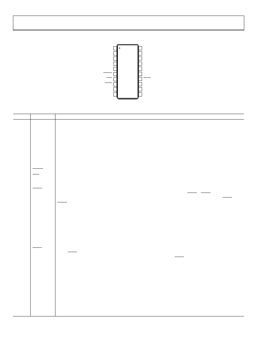
PIN CONFIGURATION AND FUNCTION DESCRIPTIONS
1
2
3
4
5
6
7
8
9
10
VOUT
VREFPS
VREFPF
CLR
RESET
VDD
INV
IOVCC
VCC
LDAC
20
19
18
17
16
15
14
13
12
11
AGND
VSS
VREFNS
SYNC
DGND
VREFNF
SDO
SDIN
SCLK
RFB
AD5791
TOP VIEW
(Not to Scale)
08964-
005
Figure 4. Pin Configuration
Table 6. Pin Function Descriptions
Pin No.
Mnemonic
Description
1
INV
Connection to Inverting Input of External Amplifier. See the AD5791 Features section for further details.
2
VOUT
Analog Output Voltage.
3
VREFPS
Positive Reference Sense Voltage Input. A voltage range of 5 V to VDD 2.5 V can be connected. A unity gain
amplifier must be connected at this pin in conjunction with the VREFPF pin. See the AD5791 Features section for
further details.
4
VREFPF
Positive Reference Force Voltage Input. A voltage range of 5 V to VDD 2.5 V can be connected. A unity gain
amplifier must be connected at this pin in conjunction with the VREFPS pin. See the AD5791 Features section for
further details.
5
VDD
Positive Analog Supply Connection. A voltage range of 7.5 V to 16.5 V can be connected, VDD should be decoupled
to AGND.
6
RESET
Active Low Reset Logic Input Pin. Asserting this pin returns the AD5791 to its power-on status.
7
CLR
Active Low Clear Logic Input Pin. Asserting this pin sets the DAC register to a user defined value (see Table 13) and
updates the DAC output. The output value depends on the DAC register coding that is being used, either binary
or twos complement.
8
LDAC
Active Low Load DAC Logic Input Pin. This is used to update the DAC register and consequently, the analog
output. When tied permanently low, the output is updated on the rising edge of SYNC. If LDAC is held high during
the write cycle, the input register is updated, but the output update is held off until the falling edge of LDAC. The
LDAC pin should not be left unconnected.
9
VCC
Digital Supply Connection. A voltage range of 2.7 V to 5.5 V can be connected. VCC should be decoupled to DGND.
10
IOVCC
Digital Interface Supply Pin. Digital threshold levels are referenced to the voltage applied to this pin. A voltage in
the range of 1.71 V to 5.5 V can be connected. IOVCC should not be allowed to exceed VCC.
11
SDO
Serial Data Output Pin. Data is clocked out on the rising edge of the serial clock input.
12
SDIN
Serial Data Input Pin. This device has a 24-bit shift register. Data is clocked into the register on the falling edge of
the serial clock input.
13
SCLK
Serial Clock Input. Data is clocked into the input shift register on the falling edge of the serial clock input. Data can
be transferred at clock rates of up to 35 MHz.
14
SYNC
Active Low Digital Interface Synchronization Input Pin. This is the frame synchronization signal for the input data.
When SYNC is low, it enables the input shift register, and data is then transferred in on the falling edges of the
following clocks. The input shift register is updated on the rising edge of SYNC.
15
DGND
Ground Reference Pin for Digital Circuitry.
16
VREFNF
Negative Reference Force Voltage Input. A voltage range of VSS + 2.5 V to 0 V can be connected. A unity gain
amplifier must be connected at this pin, in conjunction with the VREFNS pin. See the AD5791 Features section for
further details.
17
VREFNS
Negative Reference Sense Voltage Input. A voltage range of VSS + 2.5 V to 0 V can be connected. A unity gain
amplifier must be connected at this pin, in conjunction with the VREFNF pin. See the AD5791 Features section for
further details.
18
VSS
Negative Analog Supply Connection. A voltage range of 16.5 V to 2.5 V can be connected. VSS should be
decoupled to AGND.
19
AGND
Ground Reference Pin for Analog Circuitry.
20
RFB
Feedback Connection for External Amplifier. See the AD5791 Features section for further details.
相关PDF资料 |
PDF描述 |
|---|---|
| VE-J2R-EZ | CONVERTER MOD DC/DC 7.5V 25W |
| VE-J2N-EZ | CONVERTER MOD DC/DC 18.5V 25W |
| VE-J21-EZ | CONVERTER MOD DC/DC 12V 25W |
| VI-JWZ-EZ | CONVERTER MOD DC/DC 2V 10W |
| VI-JWV-EZ | CONVERTER MOD DC/DC 5.8V 25W |
相关代理商/技术参数 |
参数描述 |
|---|---|
| EVAL-AD5821AEBZ | 功能描述:BOARD EVAL FOR AD5821 RoHS:是 类别:编程器,开发系统 >> 评估板 - 数模转换器 (DAC) 系列:- 产品培训模块:Lead (SnPb) Finish for COTS Obsolescence Mitigation Program 标准包装:1 系列:- DAC 的数量:4 位数:12 采样率(每秒):- 数据接口:串行,SPI? 设置时间:3µs DAC 型:电流/电压 工作温度:-40°C ~ 85°C 已供物品:板 已用 IC / 零件:MAX5581 |
| EVAL-AD5821EBZ | 功能描述:BOARD EVALUATION FOR AD5821 RoHS:是 类别:编程器,开发系统 >> 评估板 - 数模转换器 (DAC) 系列:- 产品培训模块:Lead (SnPb) Finish for COTS Obsolescence Mitigation Program 标准包装:1 系列:- DAC 的数量:4 位数:12 采样率(每秒):- 数据接口:串行,SPI? 设置时间:3µs DAC 型:电流/电压 工作温度:-40°C ~ 85°C 已供物品:板 已用 IC / 零件:MAX5581 |
| EVAL-AD5821EBZ1 | 制造商:AD 制造商全称:Analog Devices 功能描述:120 mA, Current Sinking, 10-Bit, I2C DAC |
| EVAL-AD5930EB | 制造商:Analog Devices 功能描述:EVALUATION CONTROL BOARD I.C. - Bulk |
| EVAL-AD5930EBZ | 功能描述:BOARD EVAL FOR AD5930 RoHS:是 类别:编程器,开发系统 >> 评估演示板和套件 系列:- 标准包装:1 系列:- 主要目的:电信,线路接口单元(LIU) 嵌入式:- 已用 IC / 零件:IDT82V2081 主要属性:T1/J1/E1 LIU 次要属性:- 已供物品:板,电源,线缆,CD 其它名称:82EBV2081 |
发布紧急采购,3分钟左右您将得到回复。