- 您现在的位置:买卖IC网 > PDF目录17049 > EVAL-AD7266EDZ (Analog Devices Inc)BOARD EVAL FOR AD7266 A/D CONV PDF资料下载
参数资料
| 型号: | EVAL-AD7266EDZ |
| 厂商: | Analog Devices Inc |
| 文件页数: | 7/29页 |
| 文件大小: | 0K |
| 描述: | BOARD EVAL FOR AD7266 A/D CONV |
| 标准包装: | 1 |
| ADC 的数量: | 2 |
| 位数: | 12 |
| 采样率(每秒): | 2M |
| 数据接口: | SPI?、QSPI?、MICROWIRE? 和 DSP |
| 输入范围: | 0 ~ 5 V |
| 在以下条件下的电源(标准): | 9mW @ 3V,27mW @ 5V |
| 工作温度: | -40°C ~ 125°C |
| 已用 IC / 零件: | AD7266 |
| 已供物品: | 板 |
第1页第2页第3页第4页第5页第6页当前第7页第8页第9页第10页第11页第12页第13页第14页第15页第16页第17页第18页第19页第20页第21页第22页第23页第24页第25页第26页第27页第28页第29页
AD7266
Rev. B | Page 14 of 28
VDD
C1
D
VIN+
R1 C2
VDD
C1
D
VIN–
R1 C2
04603-015
Figure 18. Equivalent Analog Input Circuit,
Conversion Phase—Switches Open, Track Phase—Switches Closed
When no amplifier is used to drive the analog input, the source
impedance should be limited to low values. The maximum source
impedance depends on the amount of THD that can be toler-
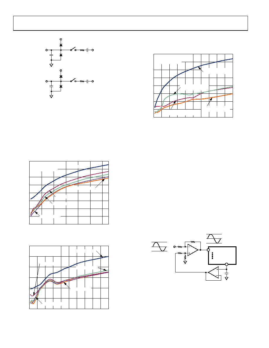
ated. The THD increases as the source impedance increases and
performance degrades. Figure 19 shows a graph of the THD vs.
the analog input signal frequency for different source impedances
in single-ended mode, while Figure 20 shows the THD vs. the
analog input signal frequency for different source impedances
in differential mode.
04
60
3-
0
16
INPUT FREQUENCY (kHz)
600
0
200
100
400
300
500
T
HD
(
d
B)
–50
–60
–55
–65
–70
–75
–80
–85
–90
FSAMPLE = 1.5MSPS
VDD = 3V
RANGE = 0V TO VREF
RSOURCE = 300
RSOURCE = 0
RSOURCE = 10
RSOURCE = 47
RSOURCE = 100
Figure 19. THD vs. Analog Input Frequency for Various
Source Impedances, Single-Ended Mode
04
60
3-
01
7
INPUT FREQUENCY (kHz)
600
700
800
900 1000
0
200
100
400
300
500
TH
D
(
d
B
)
–60
–65
–70
–75
–80
–85
–90
FSAMPLE = 1.5MSPS
VDD = 3V
RANGE = 0V TO VREF
RSOURCE = 300
RSOURCE = 0
RSOURCE = 10
RSOURCE = 47
RSOURCE = 100
Figure 20. THD vs. Analog Input Frequency for
Various Source Impedances, Differential Mode
Figure 21 shows a graph of the THD vs. the analog input
frequency for various supplies while sampling at 2 MSPS. In this
case, the source impedance is 47 Ω.
04603-018
INPUT FREQUENCY (kHz)
600
700
800
900 1000
0
200
100
400
300
500
THD
(dB)
–50
–60
–55
–65
–70
–75
–80
–85
–90
VDD = 3V
SINGLE-ENDED MODE
VDD = 5V
SINGLE-ENDED MODE
VDD = 3V
DIFFERENTIAL MODE
VDD = 5V
DIFFERENTIAL MODE
FSAMPLE = 1.5MSPS/2MSPS
VDD = 3V/5V
RANGE = 0 TO VREF
Figure 21. THD vs. Analog Input Frequency for Various Supply Voltages
ANALOG INPUTS
The AD7266 has a total of 12 analog inputs. Each on-board
ADC has six analog inputs that can be configured as six single-
ended channels, three pseudo differential channels, or three
fully differential channels. These may be selected as described
in the Analog Input Selection section.
Single-Ended Mode
The AD7266 can have a total of 12 single-ended analog input
channels. In applications where the signal source has high
impedance, it is recommended to buffer the analog input
before applying it to the ADC. The analog input range can be
programmed to be either 0 to VREF or 0 to 2 × VREF.
If the analog input signal to be sampled is bipolar, the internal
reference of the ADC can be used to externally bias up this
signal to make it correctly formatted for the ADC. Figure 22
shows a typical connection diagram when operating the ADC
in single-ended mode.
VIN
0V
+1.25V
–1.25V
DCAPA/DCAPB
VA1
AD72661
VB6
R
3R
R
0V
+2.5V
0.47F
1ADDITIONAL PINS OMITTED FOR CLARITY.
04
603
-01
9
Figure 22. Single-Ended Mode Connection Diagram
相关PDF资料 |
PDF描述 |
|---|---|
| GCM22DCSH | CONN EDGECARD 44POS DIP .156 SLD |
| 0982660859 | CBL 17POS 0.5MM JMPR TYPE A 3" |
| 0210490326 | CABLE JUMPER 1.25MM .076M 26POS |
| MAX5138EVKIT+ | EVALUATION KIT FOR MAX5138 |
| MAX5216EVKIT+ | KIT EVAL FOR MAX5214/MAX5216 |
相关代理商/技术参数 |
参数描述 |
|---|---|
| EVAL-AD7273CB | 制造商:Analog Devices 功能描述:Evaluation Board 3 MSPS,10-/12-Bit ADCs In 8-Lead TSOT 制造商:Analog Devices 功能描述:EVAL BD 3 MSPS,10-/12-BIT ADCS IN 8-LEAD TSOT - Bulk |
| EVAL-AD7273CB3 | 制造商:AD 制造商全称:Analog Devices 功能描述:3 MSPS,10-/12-Bit ADCs in 8-Lead TSOT |
| EVAL-AD7274CB | 制造商:Analog Devices 功能描述:EVAL BD 3 MSPS,10-/12-BIT ADCS IN 8-LEAD TSOT - Bulk |
| EVAL-AD7274CB3 | 制造商:AD 制造商全称:Analog Devices 功能描述:3 MSPS,10-/12-Bit ADCs in 8-Lead TSOT |
| EVAL-AD7274CBZ | 功能描述:BOARD EVALUATION FOR AD7274 RoHS:是 类别:编程器,开发系统 >> 评估板 - 模数转换器 (ADC) 系列:- 产品培训模块:Obsolescence Mitigation Program 标准包装:1 系列:- ADC 的数量:1 位数:12 采样率(每秒):94.4k 数据接口:USB 输入范围:±VREF/2 在以下条件下的电源(标准):- 工作温度:-40°C ~ 85°C 已用 IC / 零件:MAX11645 已供物品:板,软件 |
发布紧急采购,3分钟左右您将得到回复。