- 您现在的位置:买卖IC网 > PDF目录17051 > EVAL-AD7327CBZ (Analog Devices Inc)BOARD EVALUATION FOR AD7327 PDF资料下载
参数资料
| 型号: | EVAL-AD7327CBZ |
| 厂商: | Analog Devices Inc |
| 文件页数: | 2/37页 |
| 文件大小: | 0K |
| 描述: | BOARD EVALUATION FOR AD7327 |
| 标准包装: | 1 |
| 系列: | iCMOS® |
| ADC 的数量: | 1 |
| 位数: | 12 |
| 采样率(每秒): | 500k |
| 数据接口: | 串行 |
| 输入范围: | ±10 V |
| 在以下条件下的电源(标准): | 17mW @ 500kSPS |
| 工作温度: | -40°C ~ 85°C |
| 已用 IC / 零件: | AD7327 |
| 已供物品: | 板 |
| 相关产品: | AD7327BRUZ-REEL-ND - IC ADC 12BIT+SAR 8CHAN 20-TSSOP AD7327BRUZ-REEL7-ND - IC ADC 12BIT+ SAR 8CHAN 20TSSOP AD7327BRUZ-ND - IC ADC 12BIT+ SAR 8CHAN 20TSSOP |
第1页当前第2页第3页第4页第5页第6页第7页第8页第9页第10页第11页第12页第13页第14页第15页第16页第17页第18页第19页第20页第21页第22页第23页第24页第25页第26页第27页第28页第29页第30页第31页第32页第33页第34页第35页第36页第37页
Data Sheet
AD7327
Rev. B | Page 9 of 36
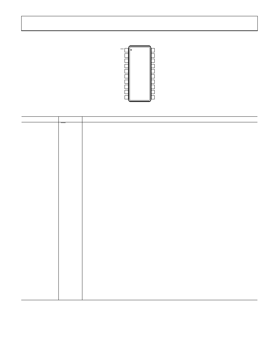
PIN CONFIGURATION AND FUNCTION DESCRIPTIONS
1
2
3
4
5
6
7
8
9
10
20
19
18
17
16
15
14
13
12
11
DIN
DGND
AGND
VIN0
VSS
REFIN/OUT
CS
DGND
DOUT
VDRIVE
VIN2
VDD
VCC
VIN5
VIN4
VIN1
VIN7
VIN6
VIN3
SCLK
AD7327
TOP VIEW
(Not to Scale)
05401-
003
Figure 3. TSSOP Pin Configuration
Table 5. Pin Function Descriptions
Pin No.
Mnemonic
Description
1
CS
Chip Select. Active low logic input. This input provides the dual function of initiating conversions on
the AD7327 and frames the serial data transfer.
2
DIN
Data In. Data to be written to the on-chip registers is provided on this input and is clocked into the
AD7327 on the falling edge of SCLK (see the Registers section).
3, 19
DGND
Digital Ground. Ground reference point for all digital circuitry on the AD7327. The DGND and AGND
voltages ideally should be at the same potential and must not be more than 0.3 V apart, even on a
transient basis.
4
AGND
Analog Ground. Ground reference point for all analog circuitry on the AD7327. All analog input signals
and any external reference signal should be referred to this AGND voltage. The AGND and DGND
voltages ideally should be at the same potential and must not be more than 0.3 V apart, even on a
transient basis.
5
REFIN/OUT
Reference Input/Reference Output. The on-chip reference is available on this pin for external use to the
AD7327. The nominal internal reference voltage is 2.5 V, which appears at this pin. A 680 nF capacitor
should be placed on the reference pin (see the Reference section). Alternatively, the internal reference
can be disabled and an external reference applied to this input. On power-up, the external reference
mode is the default condition.
6
VSS
Negative Power Supply Voltage. This is the negative supply voltage for the analog input section.
7, 8, 14, 13, 9,
10, 12, 11
VIN0 to VIN7
Analog Input 0 to Analog Input 7. The analog inputs are multiplexed into the on-chip track-and-hold.
The analog input channel for conversion is selected by programming the channel address Bit ADD2
through Bit ADD0 in the control register. The inputs can be configured as eight single-ended inputs,
four true differential input pairs, four pseudo differential inputs, or seven pseudo differential inputs.
The configuration of the analog inputs is selected by programming the mode bits, Bit Mode 1 and
Bit Mode 0, in the control register. The input range on each input channel is controlled by program-
ming the range registers. Input ranges of ±10 V, ±5 V, ±2.5 V, and 0 V to +10 V can be selected on each
analog input channel when a +2.5 V reference voltage is used (see the Registers section).
15
VDD
Positive Power Supply Voltage. This is the positive supply voltage for the analog input section.
16
VCC
Analog Supply Voltage, 2.7 V to 5.25 V. This is the supply voltage for the ADC core on the AD7327.
This supply should be decoupled to AGND.
17
VDRIVE
Logic Power Supply Input. The voltage supplied at this pin determines at what voltage the interface
operates. This pin should be decoupled to DGND. The voltage at this pin may be different to that at VCC,
but it should not exceed VCC by more than 0.3 V.
18
DOUT
Serial Data Output. The conversion output data is supplied to this pin as a serial data stream. The bits
are clocked out on the falling edge of the SCLK input, and 16 SCLKs are required to access the data. The
data stream consists of three channel identification bits, the sign bit, and 12 bits of conversion data.
The data is provided MSB first (see the Serial Interface section).
20
SCLK
Serial Clock, Logic Input. A serial clock input provides the SCLK used for accessing the data from the
AD7327. This clock is also used as the clock source for the conversion process.
相关PDF资料 |
PDF描述 |
|---|---|
| VI-BNB-EY | CONVERTER MOD DC/DC 95V 50W |
| EBC35DRYH | CONN EDGECARD 70POS DIP .100 SLD |
| VE-B1V-EY | CONVERTER MOD DC/DC 5.8V 50W |
| EVAL-AD7995EBZ | BOARD EVAL FOR AD7995 |
| AT-S-26-8/8/S-25-R | MOD CORD STANDARD 8-8 SILVER 25' |
相关代理商/技术参数 |
参数描述 |
|---|---|
| EVAL-AD7327SDZ | 功能描述:BOARD EVAL FOR AD7327SDZ RoHS:否 类别:编程器,开发系统 >> 评估板 - 模数转换器 (ADC) 系列:* 产品培训模块:Obsolescence Mitigation Program 标准包装:1 系列:- ADC 的数量:1 位数:12 采样率(每秒):94.4k 数据接口:USB 输入范围:±VREF/2 在以下条件下的电源(标准):- 工作温度:-40°C ~ 85°C 已用 IC / 零件:MAX11645 已供物品:板,软件 |
| EVAL-AD7328CB | 制造商:AD 制造商全称:Analog Devices 功能描述:8-Channel, Software-Selectable True Bipolar Input, 12-Bit Plus Sign ADC |
| EVAL-AD7328SDZ | 功能描述:BOARD EVAL FOR AD7328 RoHS:是 类别:编程器,开发系统 >> 评估板 - 模数转换器 (ADC) 系列:iCMOS® 产品培训模块:Obsolescence Mitigation Program 标准包装:1 系列:- ADC 的数量:1 位数:12 采样率(每秒):94.4k 数据接口:USB 输入范围:±VREF/2 在以下条件下的电源(标准):- 工作温度:-40°C ~ 85°C 已用 IC / 零件:MAX11645 已供物品:板,软件 |
| EVAL-AD7329CB | 制造商:Analog Devices 功能描述: |
| EVAL-AD7329CBZ | 功能描述:BOARD EVALUATION FOR AD7329CBZ RoHS:是 类别:编程器,开发系统 >> 评估板 - 模数转换器 (ADC) 系列:iCMOS® 产品培训模块:Obsolescence Mitigation Program 标准包装:1 系列:- ADC 的数量:1 位数:12 采样率(每秒):94.4k 数据接口:USB 输入范围:±VREF/2 在以下条件下的电源(标准):- 工作温度:-40°C ~ 85°C 已用 IC / 零件:MAX11645 已供物品:板,软件 |
发布紧急采购,3分钟左右您将得到回复。