- 您现在的位置:买卖IC网 > PDF目录17049 > EVAL-AD7357EDZ (Analog Devices Inc)BOARD EVAL FOR AD7357 PDF资料下载
参数资料
| 型号: | EVAL-AD7357EDZ |
| 厂商: | Analog Devices Inc |
| 文件页数: | 5/21页 |
| 文件大小: | 0K |
| 描述: | BOARD EVAL FOR AD7357 |
| 标准包装: | 1 |
| ADC 的数量: | 2 |
| 位数: | 14 |
| 采样率(每秒): | 4.2M |
| 数据接口: | 串行 |
| 输入范围: | ±VREF/2 |
| 在以下条件下的电源(标准): | 36mW @ 4.2MSPS |
| 工作温度: | -40°C ~ 85°C |
| 已用 IC / 零件: | AD7357 |
| 已供物品: | 板,CD |
AD7357
Rev. B | Page 12 of 20
THEORY OF OPERATION
CIRCUIT INFORMATION
The AD7357 is a high speed, dual, 14-bit, single-supply, successive
approximation analog-to-digital converter. The part operates
from a 2.5 V power supply and features throughput rates up to
4.2 MSPS.
The AD7357 contains two on-chip differential track-and-hold
amplifiers, two successive approximation analog-to-digital
converters, and a serial interface with two separate data output
pins. The part is housed in a 16-lead TSSOP package, offering
the user considerable space-saving advantages over alternative
solutions.
The serial clock input accesses data from the part, but also
provides the clock source for each successive approximation
ADC. The AD7357 has an on-chip 2.048 V reference. If an
external reference is desired the internal reference can be
overdriven with a reference value ranging from (2.048 V +
100 mV) to VDD. If the internal reference is to be used else-
where in the system, the reference output needs to be buffered
first. The differential analog input range for the AD7357 is VCM
± VREF/2.
The AD7357 features power-down options to allow power
saving between conversions. The power-down feature is
implemented via the standard serial interface, as described
in the Modes of Operation section.
CONVERTER OPERATION
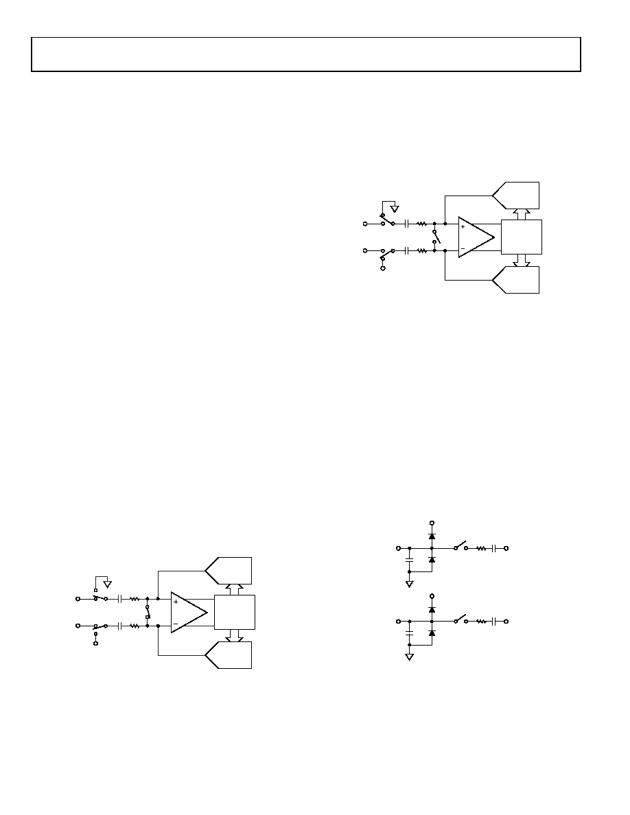
The AD7357 has two successive approximation ADCs, each
show simplified schematics of one of these ADCs in acquisition
and conversion phases, respectively. The ADC comprises
control logic, a SAR, and two capacitive DACs. In Figure 14
(the acquisition phase), SW3 is closed, SW1 and SW2 are in
Position A, the comparator is held in a balanced condition,
and the sampling capacitor arrays may acquire the differential
signal on the input.
CAPACITIVE
DAC
CAPACITIVE
DAC
CONTROL
LOGIC
COMPARATOR
SW3
SW1
A
B
SW2
CS
VIN+
VIN–
VREF
0
77
57-
01
3
Figure 14. ADC Acquisition Phase
When the ADC starts a conversion (see Figure 15), SW3 opens
and SW1 and SW2 move to Position B, causing the comparator
to become unbalanced. Both inputs are disconnected when the
conversion begins. The control logic and charge redistribution
DACs are used to add and subtract fixed amounts of charge
from the sampling capacitor arrays to bring the comparator
back into a balanced condition. When the comparator is
rebalanced, the conversion is complete. The control logic
generates the ADC output code. The output impedances of
the sources driving the VIN+ and VIN pins must be matched;
otherwise, the two inputs have different settling times, resulting
in errors.
CAPACITIVE
DAC
CAPACITIVE
DAC
CONTROL
LOGIC
COMPARATOR
SW3
SW1
A
B
SW2
CS
VIN+
VIN–
VREF
07
75
7-
0
14
Figure 15. ADC Conversion Phase
ANALOG INPUT STRUCTURE
Figure 16 shows the equivalent circuit of the analog input struc-
ture of the AD7357. The four diodes provide ESD protection for
the analog inputs. Care must be taken to ensure that the analog
input signals never exceed the supply rails by more than 300 mV.
Exceeding the limit causes these diodes to become forward-
biased and start conducting into the substrate. These diodes
can conduct up to 10 mA without causing irreversible damage
to the part.
The C1 capacitors in Figure 16 are typically 8 pF and can
primarily be attributed to pin capacitance. The R1 resistors
are lumped components made up of the on resistance of the
switches. The value of these resistors is typically about 30 Ω.
The C2 capacitors are the ADC’s sampling capacitors with a
capacitance of 32 pF typically.
VDD
C1
D
VIN+
R1 C2
VDD
C1
D
VIN–
R1 C2
07
75
7-
0
15
Figure 16. Equivalent Analog Input Circuit,
Conversion Phase—Switches Open, Track Phase—Switches Closed
相关PDF资料 |
PDF描述 |
|---|---|
| ECE-A0JKG220 | CAP ALUM 22UF 6.3V 20% RADIAL |
| GEM25DTAH | CONN EDGECARD 50POS R/A .156 SLD |
| STD09W-Q | WIRE & CABLE MARKERS |
| ISL5761EVAL1 | EVALUATION PLATFORM ISL5761 SOIC |
| STD02W-M | WIRE & CABLE MARKERS |
相关代理商/技术参数 |
参数描述 |
|---|---|
| EVAL-AD7366CBZ | 功能描述:BOARD EVALUATION FOR AD7366 RoHS:是 类别:编程器,开发系统 >> 评估板 - 模数转换器 (ADC) 系列:iCMOS® 产品培训模块:Obsolescence Mitigation Program 标准包装:1 系列:- ADC 的数量:1 位数:12 采样率(每秒):94.4k 数据接口:USB 输入范围:±VREF/2 在以下条件下的电源(标准):- 工作温度:-40°C ~ 85°C 已用 IC / 零件:MAX11645 已供物品:板,软件 |
| EVAL-AD7366SDZ | 功能描述:BOARD EVAL FOR AD7366 RoHS:是 类别:编程器,开发系统 >> 评估板 - 模数转换器 (ADC) 系列:iCMOS® 产品培训模块:Obsolescence Mitigation Program 标准包装:1 系列:- ADC 的数量:1 位数:12 采样率(每秒):94.4k 数据接口:USB 输入范围:±VREF/2 在以下条件下的电源(标准):- 工作温度:-40°C ~ 85°C 已用 IC / 零件:MAX11645 已供物品:板,软件 |
| EVAL-AD7367CBZ | 制造商:AD 制造商全称:Analog Devices 功能描述:True Bipolar Input, Dual 1 レs, 12-/14-Bit, 2-Channel SAR ADCs |
| EVAL-AD7367SDZ | 功能描述:数据转换 IC 开发工具 EVALUATION CONTROL BOARD I.C. RoHS:否 制造商:Texas Instruments 产品:Demonstration Kits 类型:ADC 工具用于评估:ADS130E08 接口类型:SPI 工作电源电压:- 6 V to + 6 V |
| EVAL-AD7376EBZ | 功能描述:BOARD EVAL FOR AD7376 RoHS:是 类别:编程器,开发系统 >> 评估演示板和套件 系列:- 标准包装:1 系列:- 主要目的:电信,线路接口单元(LIU) 嵌入式:- 已用 IC / 零件:IDT82V2081 主要属性:T1/J1/E1 LIU 次要属性:- 已供物品:板,电源,线缆,CD 其它名称:82EBV2081 |
发布紧急采购,3分钟左右您将得到回复。