- 您现在的位置:买卖IC网 > PDF目录17048 > EVAL-AD7451CBZ (Analog Devices Inc)BOARD EVAL FOR AD7451 PDF资料下载
参数资料
| 型号: | EVAL-AD7451CBZ |
| 厂商: | Analog Devices Inc |
| 文件页数: | 8/25页 |
| 文件大小: | 0K |
| 描述: | BOARD EVAL FOR AD7451 |
| 标准包装: | 1 |
| ADC 的数量: | 1 |
| 位数: | 12 |
| 采样率(每秒): | 1M |
| 数据接口: | SPI?、QSPI?、MICROWIRE? 和 DSP |
| 输入范围: | ±VREF |
| 在以下条件下的电源(标准): | 9.25mW @ 1MSPS,5V |
| 工作温度: | -40°C ~ 85°C |
| 已用 IC / 零件: | AD7451 |
| 已供物品: | 板 |
AD7441/AD7451
Rev. D | Page 15 of 24
When no amplifier is used to drive the analog input, it is
recommended that the source impedance be limited to low
values. The maximum source impedance depends on the
amount of total harmonic distortion that can be tolerated.
The THD increases as the source impedance increases and
performance degrades.
Figure 25 shows a graph of THD vs. analog input signal
frequency for different source impedances.
0
–100
–90
–80
–70
–60
–50
–40
–30
–10
–20
10k
100k
1M
INPUT FREQUENCY (Hz)
T
H
D
(
d
B)
200
100
62
10
TA = 25°C
VDD = 5V
03
15
3
-02
5
Figure 25. THD vs. Analog Input Frequency for Various Source Impedances
Figure 26 shows a graph of THD vs. analog input frequency for
various supply voltages while sampling at 1 MSPS with an SCLK
of 18 MHz. In this case, the source impedance is 10 Ω.
–50
–90
–85
–80
–75
–70
–65
–60
–55
10
100
1000
INPUT FREQUENCY (kHz)
T
H
D
(
d
B)
TA = 25°C
VDD = 2.7V
VDD = 3.6V
VDD = 4.75V
VDD = 5.25V
03
15
3
-02
6
Figure 26. THD vs. Analog Input Frequency for Various Supply Voltages
DIGITAL INPUTS
The digital inputs applied to the AD7441/AD7451 are not limited
by the maximum ratings that limit the analog inputs. Instead,
the digital inputs applied, that is, CS and SCLK, can go to 7 V
and are not restricted by the VDD + 0.3 V limits as on the analog
input. The main advantage of the inputs not being restricted to
the VDD + 0.3 V limit is that power supply sequencing issues are
avoided. If CS or SCLK are applied before VDD, there is no risk
of latch-up as there would be on the analog inputs if a signal
greater than 0.3 V were applied prior to VDD.
REFERENCE
An external source is required to supply the reference to the
AD7441/AD7451. This reference input can range from 100 mV
to VDD. The specified reference is 2.5 V for the power supply
range 2.7 V to 5.25 V. The reference input chosen for an appli-
cation must never be greater than the power supply. Errors in
the reference source result in gain errors in the AD7441/AD7451
transfer function and add to the specified full-scale errors of the
part. A capacitor of at least 0.1 μF must be placed on the VREF
pin. Suitable reference sources for the AD7441/AD7451 include
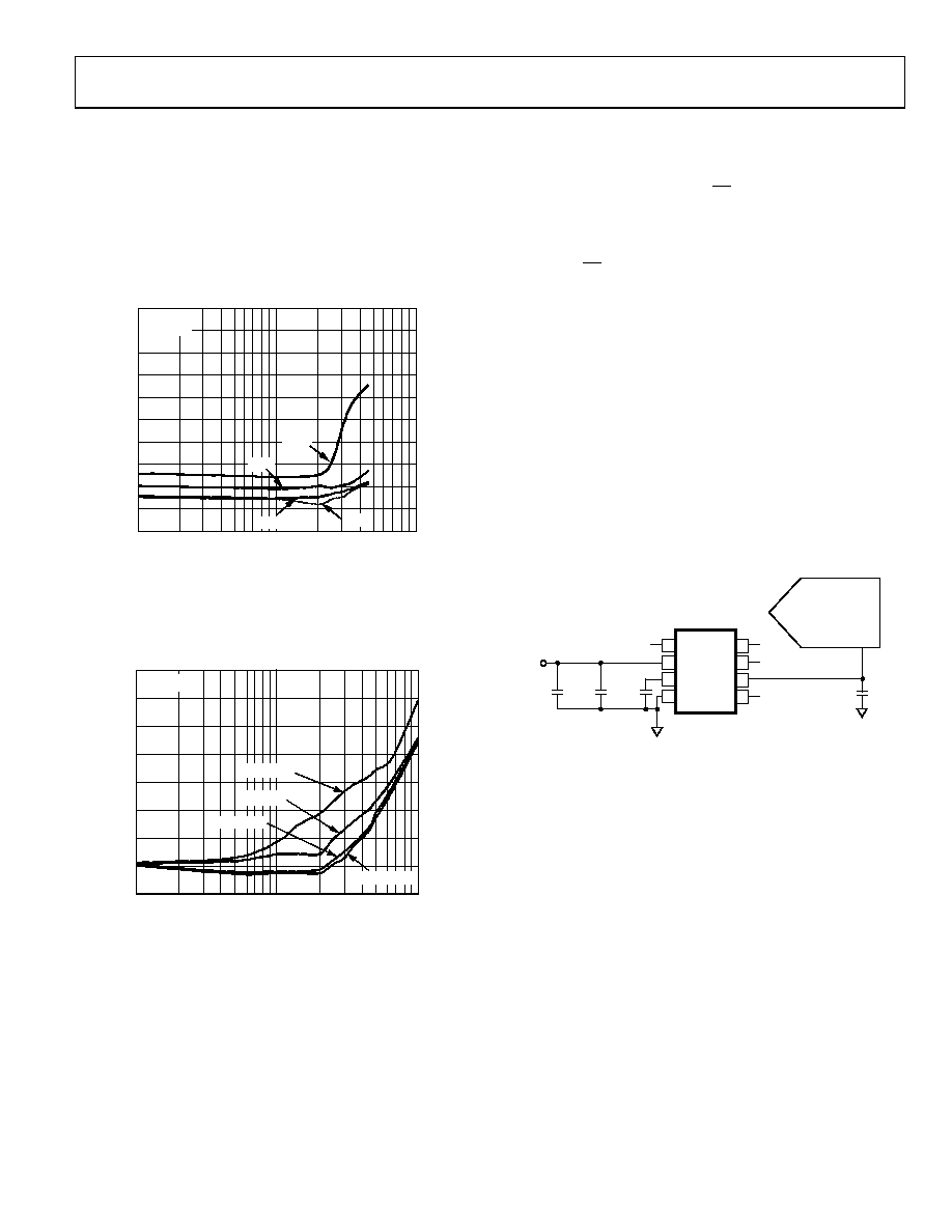
tion diagram for the VREF pin.
1
AD780
NC
8
2
VIN
NC
7
3
GND
6
4
TEMP
5
OPSEL
TRIM
VOUT
AD7441/
AD7451*
VREF
2.5V
NC
VDD
NC
VDD
NC = NO CONNECT
10nF
0.1F
*ADDITIONAL PINS OMITTED FOR CLARITY.
0
31
53
-0
27
Figure 27. Typical VREF Connection Diagram for VDD = 5 V
相关PDF资料 |
PDF描述 |
|---|---|
| STD02W-T | WIRE & CABLE MARKERS |
| STD09W-J | WIRE & CABLE MARKERS |
| HKQ0603S0N8C-T | INDUCTOR HI FREQ 0.8NH 0201 |
| STD01W-G | WIRE & CABLE MARKERS |
| EVAL-AD7949EDZ | BOARD EVAL AD7949 |
相关代理商/技术参数 |
参数描述 |
|---|---|
| EVAL-AD7451CBZ3 | 制造商:AD 制造商全称:Analog Devices 功能描述:Pseudo Differential Input, 1 MSPS, 10-/12-Bit ADCs in an 8-Lead SOT-23 |
| EVAL-AD7452CB | 制造商:Analog Devices 功能描述:DEV TOOLS, DIFFERENTIAL INPUT, 555KSPS, 12BIT ADC IN AN 8-LE - Bulk |
| EVAL-AD7452CB3 | 制造商:AD 制造商全称:Analog Devices 功能描述:Differential Input, 555 kSPS 12-Bit ADC in an 8-Lead SOT-23 |
| EVAL-AD7453CB | 制造商:Analog Devices 功能描述:DEV TOOLS, PSEUDO DIFFERENTIAL, 555 KSPS, 12-BIT A/D CNVRTR - Bulk |
| EVAL-AD7453CB2 | 制造商:AD 制造商全称:Analog Devices 功能描述:Pseudo Differential, 555 kSPS, 12-Bit ADC in an 8-Lead SOT-23 |
发布紧急采购,3分钟左右您将得到回复。