- 您现在的位置:买卖IC网 > PDF目录17045 > EVAL-AD7606-4EDZ (Analog Devices Inc)EVAL BOARD FOR AD7606 PDF资料下载
参数资料
| 型号: | EVAL-AD7606-4EDZ |
| 厂商: | Analog Devices Inc |
| 文件页数: | 16/36页 |
| 文件大小: | 0K |
| 描述: | EVAL BOARD FOR AD7606 |
| 标准包装: | 1 |
| ADC 的数量: | 1 |
| 位数: | 16 |
| 采样率(每秒): | 200k |
| 数据接口: | DSP,MICROWIRE?,QSPI?,串行,SPI? |
| 在以下条件下的电源(标准): | 75mW @ 200kSPS |
| 工作温度: | -40°C ~ 85°C |
| 已用 IC / 零件: | AD7606-4 |
| 已供物品: | 板 |
第1页第2页第3页第4页第5页第6页第7页第8页第9页第10页第11页第12页第13页第14页第15页当前第16页第17页第18页第19页第20页第21页第22页第23页第24页第25页第26页第27页第28页第29页第30页第31页第32页第33页第34页第35页第36页
Data Sheet
AD7606/AD7606-6/AD7606-4
Rev. C | Page 23 of 36
1M
CLAMP
Vx
1M
CLAMP
VxGND
RFB
C
R
ANALOG
INPUT
SIGNAL
AD7606
0
847
9-
0
34
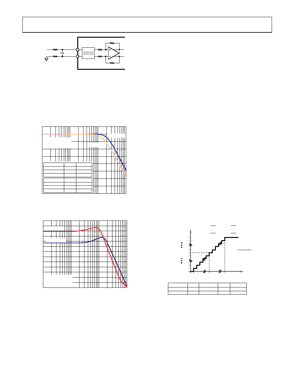
Figure 36. Input Resistance Matching on the Analog Input of the
AD7606/AD7606-6/AD7606-4
Analog Input Antialiasing Filter
An analog antialiasing filter (a second-order Butterworth) is also
provided on the AD7606/AD7606-6/AD7606-4. Figure 37 and
Figure 38 show the frequency and phase response, respectively,
of the analog antialiasing filter. In the ±5 V range, the 3 dB
frequency is typically 15 kHz. In the ±10 V range, the 3 dB
frequency is typically 23 kHz.
5
0
–5
–10
–15
–20
–25
–30
–35
–40
100
1k
10k
100k
AT
T
E
N
UAT
IO
N
(
d
B
)
INPUT FREQUENCY (Hz)
08
47
9-
0
35
±10V RANGE
±5V RANGE
AVCC, VDRIVE = 5V
FSAMPLE = 200kSPS
TA = 25°C
±10V RANGE
0.1dB
3dB
–40
10,303
24,365Hz
+25
9619
23,389Hz
+85
9326
22,607Hz
±5V RANGE
0.1dB
3dB
–40
5225
16,162Hz
+25
5225
15,478Hz
+85
4932
14,990Hz
Figure 37. Analog Antialiasing Filter Frequency Response
18
16
14
12
10
8
6
4
2
0
–2
–4
–6
10
100k
10k
1k
–8
P
HAS
E
D
E
L
A
Y
(
s)
INPUT FREQUENCY (Hz)
08
47
9-
0
36
AVCC, VDRIVE = 5V
FSAMPLE = 200kSPS
TA = 25°C
±5V RANGE
±10V RANGE
Figure 38. Analog Antialias Filter Phase Response
Track-and-Hold Amplifiers
The track-and-hold amplifiers on the AD7606/AD7606-6/
AD7606-4 allow the ADC to accurately acquire an input sine wave
of full-scale amplitude to 16-bit resolution. The track-and-hold
amplifiers sample their respective inputs simultaneously on the
rising edge of CONVST x. The aperture time for the track-and-
hold (that is, the delay time between the external CONVST x
signal and the track-and-hold actually going into hold) is well
matched, by design, across all eight track-and-holds on one
device and from device to device. This matching allows more
than one AD7606/AD7606-6/AD7606-4 device to be sampled
simultaneously in a system.
The end of the conversion process across all eight channels is
indicated by the falling edge of BUSY; and it is at this point that the
track-and-holds return to track mode, and the acquisition time
for the next set of conversions begins.
The conversion clock for the part is internally generated, and
the conversion time for all channels is 4 μs on the AD7606,
3 μs on the AD7606-6, and 2 μs on the AD7606-4. On the AD7606,
the BUSY signal returns low after all eight conversions to indicate
the end of the conversion process. On the falling edge of BUSY,
the track-and-hold amplifiers return to track mode. New data
can be read from the output register via the parallel, parallel
byte, or serial interface after BUSY goes low; or, alternatively,
data from the previous conversion can be read while BUSY is
high. Reading data from the AD7606/AD7606-6/AD7606-4
while a conversion is in progress has little effect on performance
and allows a faster throughput to be achieved. In parallel mode
at VDRIVE > 3.3 V, the SNR is reduced by ~1.5 dB when reading
during a conversion.
ADC TRANSFER FUNCTION
The output coding of the AD7606/AD7606-6/AD7606-4 is
twos complement. The designed code transitions occur midway
between successive integer LSB values, that is, 1/2 LSB and 3/2 LSB.
The LSB size is FSR/65,536 for the AD7606. The ideal transfer
characteristic for the AD7606/AD7606-6/AD7606-4 is shown
011...111
011...110
000...001
000...000
111...111
100...010
100...001
100...000
–FS + 1/2LSB 0V – 1/2LSB +FS – 3/2LSB
A
DC
CO
DE
ANALOG INPUT
+FS
MIDSCALE
–FS
LSB
±10V RANGE +10V
0V
–10V
305V
±5V RANGE
+5V
0V
–5V
152V
+FS – (–FS)
216
LSB =
VIN
5V
REF
2.5V
±5V CODE =
× 32,768 ×
VIN
10V
REF
2.5V
±10V CODE =
× 32,768 ×
08
47
9-
03
7
Figure 39. AD7606/AD7606-6/AD7606-4 Transfer Characteristics
The LSB size is dependent on the analog input range selected.
相关PDF资料 |
PDF描述 |
|---|---|
| VI-BWX-EY | CONVERTER MOD DC/DC 5.2V 50W |
| STD02W-N | WIRE & CABLE MARKERS |
| VI-BWW-EY | CONVERTER MOD DC/DC 5.5V 50W |
| EVAL-AD7983SDZ | BOARD EVAL FOR AD7983 |
| VI-BW0-EY | CONVERTER MOD DC/DC 5V 50W |
相关代理商/技术参数 |
参数描述 |
|---|---|
| EVAL-AD7606-6EDZ | 功能描述:EVAL BOARD FOR AD7606 RoHS:是 类别:编程器,开发系统 >> 评估板 - 模数转换器 (ADC) 系列:- 产品培训模块:Obsolescence Mitigation Program 标准包装:1 系列:- ADC 的数量:1 位数:12 采样率(每秒):94.4k 数据接口:USB 输入范围:±VREF/2 在以下条件下的电源(标准):- 工作温度:-40°C ~ 85°C 已用 IC / 零件:MAX11645 已供物品:板,软件 |
| EVAL-AD7606EDZ | 功能描述:EVAL BOARD FOR AD7606 RoHS:是 类别:编程器,开发系统 >> 评估板 - 模数转换器 (ADC) 系列:- 产品培训模块:Obsolescence Mitigation Program 标准包装:1 系列:- ADC 的数量:1 位数:12 采样率(每秒):94.4k 数据接口:USB 输入范围:±VREF/2 在以下条件下的电源(标准):- 工作温度:-40°C ~ 85°C 已用 IC / 零件:MAX11645 已供物品:板,软件 |
| EVAL-AD7607EDZ | 功能描述:EVAL BOARD FOR AD7607 RoHS:是 类别:编程器,开发系统 >> 评估板 - 模数转换器 (ADC) 系列:- 产品培训模块:Obsolescence Mitigation Program 标准包装:1 系列:- ADC 的数量:1 位数:12 采样率(每秒):94.4k 数据接口:USB 输入范围:±VREF/2 在以下条件下的电源(标准):- 工作温度:-40°C ~ 85°C 已用 IC / 零件:MAX11645 已供物品:板,软件 |
| EVAL-AD7608EDZ | 功能描述:BOARD EVAL FOR AD7608 RoHS:是 类别:编程器,开发系统 >> 评估板 - 模数转换器 (ADC) 系列:- 产品培训模块:Obsolescence Mitigation Program 标准包装:1 系列:- ADC 的数量:1 位数:12 采样率(每秒):94.4k 数据接口:USB 输入范围:±VREF/2 在以下条件下的电源(标准):- 工作温度:-40°C ~ 85°C 已用 IC / 零件:MAX11645 已供物品:板,软件 |
| EVAL-AD7609EDZ | 功能描述:BOARD EVAL FOR AD7609 RoHS:是 类别:编程器,开发系统 >> 评估板 - 模数转换器 (ADC) 系列:- 产品培训模块:Obsolescence Mitigation Program 标准包装:1 系列:- ADC 的数量:1 位数:12 采样率(每秒):94.4k 数据接口:USB 输入范围:±VREF/2 在以下条件下的电源(标准):- 工作温度:-40°C ~ 85°C 已用 IC / 零件:MAX11645 已供物品:板,软件 |
发布紧急采购,3分钟左右您将得到回复。