- 您现在的位置:买卖IC网 > PDF目录17036 > EVAL-AD7607EDZ (Analog Devices Inc)EVAL BOARD FOR AD7607 PDF资料下载
参数资料
| 型号: | EVAL-AD7607EDZ |
| 厂商: | Analog Devices Inc |
| 文件页数: | 11/32页 |
| 文件大小: | 0K |
| 描述: | EVAL BOARD FOR AD7607 |
| 标准包装: | 1 |
| ADC 的数量: | 1 |
| 位数: | 14 |
| 采样率(每秒): | 200k |
| 数据接口: | DSP,MICROWIRE?,QSPI?,串行,SPI? |
| 在以下条件下的电源(标准): | 80mW @ 200kSPS |
| 工作温度: | -40°C ~ 85°C |
| 已用 IC / 零件: | AD7607 |
| 已供物品: | 板 |
第1页第2页第3页第4页第5页第6页第7页第8页第9页第10页当前第11页第12页第13页第14页第15页第16页第17页第18页第19页第20页第21页第22页第23页第24页第25页第26页第27页第28页第29页第30页第31页第32页
Data Sheet
AD7607
Rev. B | Page 19 of 32
THEORY OF OPERATION
CONVERTER DETAILS
The AD7607 is a data acquisition system that employs a high
speed, low power, charge redistribution, successive approxi-
mation analog-to-digital converter (ADC) and allows the
simultaneous sampling of eight analog input channels. The analog
inputs on the AD7607 can accept true bipolar input signals. The
RANGE pin is used to select either ±10 V or ±5 V as the input
range. The AD7607 operates from a single 5 V supply.
The AD7607 contains input clamp protection, input signal scaling
amplifiers, a second-order antialiasing filter, track-and-hold
amplifiers, an on-chip reference, reference buffers, a high speed
ADC, a digital filter, and high speed parallel and serial interfaces.
Sampling on the AD7607 is controlled using the CONVST signals.
ANALOG INPUT
Analog Input Ranges
The AD7607 can handle true bipolar input voltages. The logic
level on the RANGE pin determines the analog input range of
all analog input channels. If this pin is tied to a logic high, the
analog input range is ±10 V for all channels. If this pin is tied
to a logic low, the analog input range is ±5 V for all channels.
A logic change on this pin has an immediate effect on the analog
input range; however, there is a typical settling time of ~80 s,
in addition to the normal acquisition time requirement.
Recommended practice is to hardwire the RANGE pin
according to the desired input range for the system signals.
During normal operation, the applied analog input voltage should
remain within the analog input range selected via the range pin.
A RESET pulse must be applied after power-up to ensure the
analog input channels are configured for the range selected.
When in a power-down mode, it is recommended to tie the
analog inputs to GND. As per the input clamp protection section,
the overvoltage clamp protection is recommended for use in
transient overvoltage conditions and should not remain active
for extended periods. Stressing the analog inputs outside of the
conditions mentioned here may degrade the Bipolar Zero Code
error and THD performance of the AD7607.
Analog Input Impedance
The analog input impedance of the AD7607 is 1 M. This is
a fixed input impedance that does not vary with the AD7607
sampling frequency. This high analog input impedance elimi-
nates the need for a driver amplifier in front of the AD7607,
allowing for direct connection to the source or sensor. With the
need for a driver amplifier eliminated, bipolar supplies (which
are often a source of noise in a system) can be removed from
the signal chain.
Analog Input Clamp Protection
Figure 30 shows the analog input structure of the AD7607.
Each AD7607 analog input contains clamp protection circuitry.
Despite single 5 V supply operation, this analog input clamp
protection allows for an input overvoltage of up to ±16.5 V.
08096-
032
1M
CLAMP
Vx
1M
CLAMP
VxGND
SECOND-
ORDER
LPF
RFB
Figure 30. Analog Input Circuitry
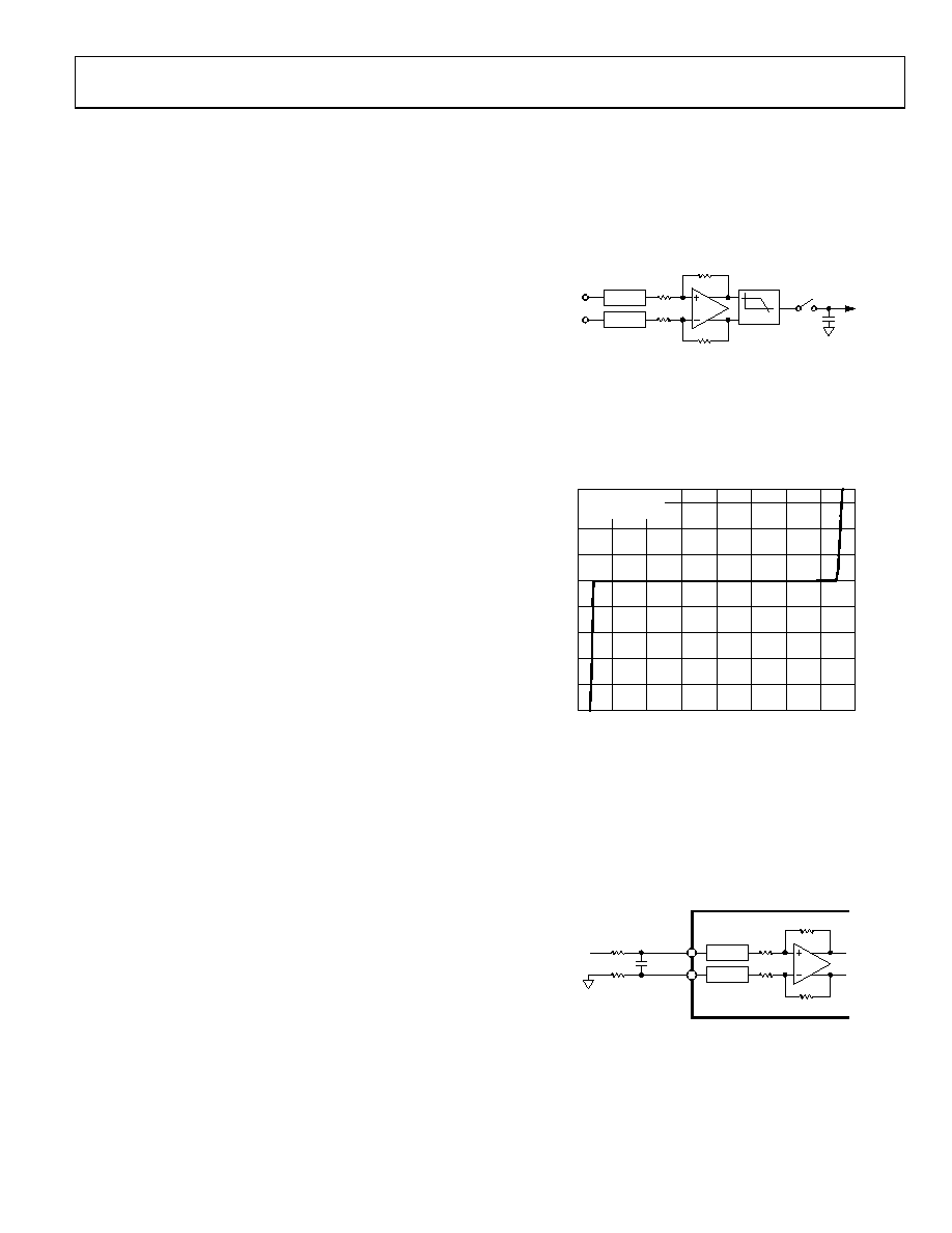
Figure 31 shows the voltage vs. current characteristic of the
clamp circuit. For input voltages of up to ±16.5 V, no current
flows in the clamp circuit. For input voltages that are above ±16.5 V,
the AD7607 clamp circuitry turns on and clamps the analog
input to ±16.5 V.
30
–50
–40
–30
–20
–10
0
10
20
–20
–15
–10
–5
0
5
10
15
20
INP
UT
CL
AM
P
CURRE
NT
(
mA)
SOURCE VOLTAGE (V)
08096-
051
AVCC, VDRIVE = 5V
TA = 25°C
Figure 31. Input Protection Clamp Profile
A series resistor should be placed on the analog input channels
to limit the current to ±10 mA for input voltages above ±16.5 V.
In an application where there is a series resistance on an analog
input channel, Vx, a corresponding resistance is required on the
analog input GND channel, VxGND (see Figure 32). If there is
no corresponding resistor on the VxGND channel, an offset
error occurs on that channel.
1M
CLAMP
VINx
1M
CLAMP
VxGND
RFB
C
R
ANALOG
INPUT
SIGNAL
AD7607
08096-
032
Figure 32. Input Resistance Matching on the Analog Input
相关PDF资料 |
PDF描述 |
|---|---|
| GSC12DRTS-S13 | CONN EDGECARD 24POS .100 EXTEND |
| GMC12DRTS-S13 | CONN EDGECARD 24POS .100 EXTEND |
| 0210490306 | CABLE JUMPER 1.25MM .102M 24POS |
| 0210490305 | CABLE JUMPER 1.25MM .102M 24POS |
| VI-B54-EY | CONVERTER MOD DC/DC 48V 50W |
相关代理商/技术参数 |
参数描述 |
|---|---|
| EVAL-AD7608EDZ | 功能描述:BOARD EVAL FOR AD7608 RoHS:是 类别:编程器,开发系统 >> 评估板 - 模数转换器 (ADC) 系列:- 产品培训模块:Obsolescence Mitigation Program 标准包装:1 系列:- ADC 的数量:1 位数:12 采样率(每秒):94.4k 数据接口:USB 输入范围:±VREF/2 在以下条件下的电源(标准):- 工作温度:-40°C ~ 85°C 已用 IC / 零件:MAX11645 已供物品:板,软件 |
| EVAL-AD7609EDZ | 功能描述:BOARD EVAL FOR AD7609 RoHS:是 类别:编程器,开发系统 >> 评估板 - 模数转换器 (ADC) 系列:- 产品培训模块:Obsolescence Mitigation Program 标准包装:1 系列:- ADC 的数量:1 位数:12 采样率(每秒):94.4k 数据接口:USB 输入范围:±VREF/2 在以下条件下的电源(标准):- 工作温度:-40°C ~ 85°C 已用 IC / 零件:MAX11645 已供物品:板,软件 |
| EVAL-AD7610CB | 制造商:Analog Devices 功能描述:EVAL KIT FOR 16BIT, 250 KSPS, UNIPOLAR/BIPOLAR PROGRAMMABLE - Bulk |
| EVAL-AD7610CBZ | 功能描述:BOARD EVALUATION FOR AD7610 RoHS:是 类别:编程器,开发系统 >> 评估板 - 模数转换器 (ADC) 系列:PulSAR® 产品培训模块:Obsolescence Mitigation Program 标准包装:1 系列:- ADC 的数量:1 位数:12 采样率(每秒):94.4k 数据接口:USB 输入范围:±VREF/2 在以下条件下的电源(标准):- 工作温度:-40°C ~ 85°C 已用 IC / 零件:MAX11645 已供物品:板,软件 |
| EVAL-AD7610EDZ | 功能描述:BOARD EVAL FOR AD7610 RoHS:是 类别:编程器,开发系统 >> 评估板 - 模数转换器 (ADC) 系列:* 产品培训模块:Obsolescence Mitigation Program 标准包装:1 系列:- ADC 的数量:1 位数:12 采样率(每秒):94.4k 数据接口:USB 输入范围:±VREF/2 在以下条件下的电源(标准):- 工作温度:-40°C ~ 85°C 已用 IC / 零件:MAX11645 已供物品:板,软件 |
发布紧急采购,3分钟左右您将得到回复。