- 您现在的位置:买卖IC网 > PDF目录17039 > EVAL-AD7660CBZ (Analog Devices Inc)BOARD EVALUATION FOR AD7660 PDF资料下载
参数资料
| 型号: | EVAL-AD7660CBZ |
| 厂商: | Analog Devices Inc |
| 文件页数: | 5/20页 |
| 文件大小: | 0K |
| 描述: | BOARD EVALUATION FOR AD7660 |
| 标准包装: | 1 |
| 系列: | PulSAR® |
| ADC 的数量: | 1 |
| 位数: | 16 |
| 采样率(每秒): | 100k |
| 数据接口: | 串行,并联 |
| 输入范围: | ±VREF |
| 在以下条件下的电源(标准): | 200mW @ 100kSPS |
| 工作温度: | -40°C ~ 85°C |
| 已用 IC / 零件: | AD7660 |
| 已供物品: | 板 |
| 相关产品: | AD7660ASTZ-ND - IC ADC 16BIT UNIPOLAR 48-LQFP AD7660ASTZRL-ND - IC ADC 16BIT UNIPOLAR 48LQFP AD7660ACPZRLTR-ND - IC ADC 16BIT UNIPOLAR 48LFCSP |
REV. D
AD7660
–13–
The AD8519, OP162, or the OP184 meet these requirements
and are usually appropriate for almost all applications. As an
alternative, in very high speed and noise-sensitive applications,
the AD8021 with an external compensation capacitor of 10 pF
or the AD829 with an external compensation capacitor of 82 pF
can be used. This capacitor should have good linearity as an
NPO ceramic or mica type. Moreover, the use of a noninverting
+1 gain arrangement is recommended and helps to obtain the
best signal-to-noise ratio.
Voltage Reference Input
The AD7660 uses an external 2.5 V voltage reference.
The voltage reference input REF of the AD7660 has a dynamic
input impedance; it should therefore be driven by a low impedance
source with an efficient decoupling between REF and REFGND
inputs. This decoupling depends on the choice of the voltage
reference but usually consists of a 1
mF ceramic capacitor and a
low ESR tantalum capacitor connected to the REF and REFGND
inputs with minimum parasitic inductance. 47
mF is an appropriate
value for the tantalum capacitor when used with one of the
recommended reference voltages:
∑ The low noise, low temperature drift ADR421 and AD780
voltage references
∑ The low power ADR291 voltage reference
∑ The low cost AD1582 voltage reference
For applications using multiple AD7660s, it is more effective to
buffer the reference voltage with a low noise, very stable op amp
like the AD8031.
Care should also be taken with the reference temperature coeffi-
cient of the voltage reference that directly affects the full-scale
accuracy if this parameter matters. For instance, a
±15 ppm/∞C
tempco of the reference changes the full scale by
±1 LSB/∞C.
VREF , as mentioned in the specification table, could be increased
to AVDD – 1.85 V. The benefit here is the increased SNR
obtained as a result of this increase. Since the input range is
defined in terms of VREF, this would essentially increase the
range to make it a
±3 V input range with an AVDD above 4.85 V.
The theoretical improvement as a result of this increase in
reference is 1.58 dB (20 log [3/2.5]). Due to the theoretical
quantization noise, however, the observed improvement is
approximately 1 dB. The AD780 can be selected with a 3 V
reference voltage.
Power Supply
The AD7660 uses three sets of power supply pins: an analog 5 V
supply AVDD, a digital 5 V core supply DVDD, and a digital
input/output interface supply OVDD. The OVDD supply allows
direct interface with any logic working between 2.7 V and 5.25 V.
To reduce the number of supplies needed, the digital core
(DVDD) can be supplied through a simple RC filter from the
analog supply, as shown in Figure 5. The AD7660 is independent
of power supply sequencing and thus free from supply voltage
induced latch-up. Additionally, it is very insensitive to power supply
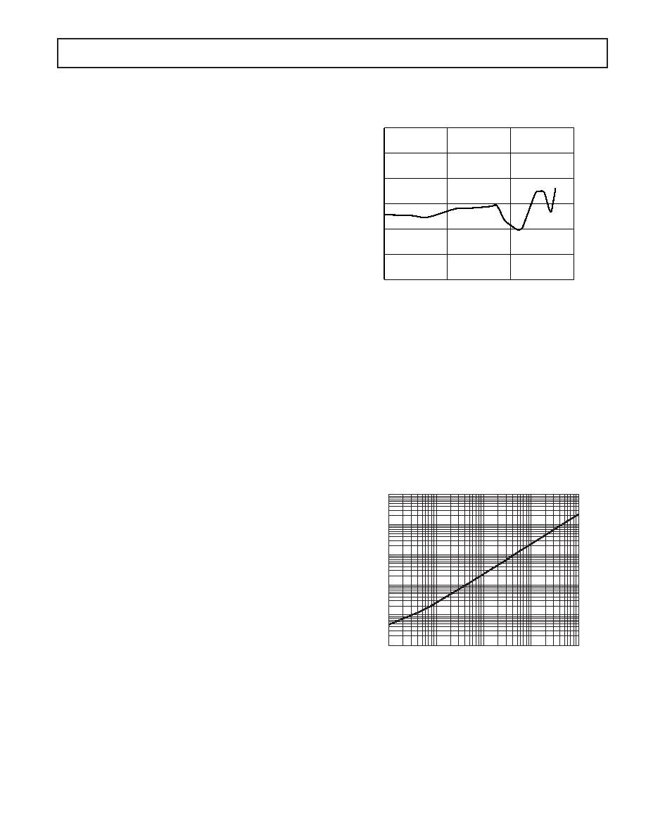
variations over a wide frequency range, as shown in Figure 9.
INPUT FREQUENCY – Hz
PSRR
–
dB
–80
1k
10k
100k
1M
–75
–70
–65
–60
–55
–50
Figure 9. PSRR vs. Frequency
POWER DISSIPATION VS. THROUGHPUT
The AD7660 automatically reduces its power consumption at
the end of each conversion phase. During the acquisition phase,
the operating currents are very low, which allows a significant
power saving when the conversion rate is reduced, as shown in
Figure 10. This feature makes the AD7660 ideal for very low
power battery applications. It should be noted that the digital
interface remains active even during the acquisition phase. To
reduce the operating digital supply currents even further, the
digital inputs need to be driven close to the power rails (i.e.,
DVDD and DGND for all inputs except EXT/
INT, INVSYNC,
INVSCLK, RDC/SDIN, and OVDD or OGND for the last
four inputs.
THROUGHPUT – SPS
10
100000
POWER
DISSIPATION
–
W
100000
1000
10000
100
1
10
100
1000
10000
Figure 10. Power Dissipation vs. Sample Rate
相关PDF资料 |
PDF描述 |
|---|---|
| MPC8379E-RDB | BOARD REFERENCE FOR MPC837 |
| MPC8379E-MDS-PB | BOARD PROCESSOR FOR MDS S |
| MPC8378E-MDS-PB | BOARD PROCESSOR FOR MDS S |
| MPC5553EVBE | BOARD EVAL FOR MPC5553 |
| MPC8323E-MDS-PB | BOARD MODULE DEV SYSTEM 8323 |
相关代理商/技术参数 |
参数描述 |
|---|---|
| EVAL-AD7660EDZ | 功能描述:BOARD EVAL FOR AD7660 RoHS:是 类别:编程器,开发系统 >> 评估板 - 模数转换器 (ADC) 系列:* 产品培训模块:Obsolescence Mitigation Program 标准包装:1 系列:- ADC 的数量:1 位数:12 采样率(每秒):94.4k 数据接口:USB 输入范围:±VREF/2 在以下条件下的电源(标准):- 工作温度:-40°C ~ 85°C 已用 IC / 零件:MAX11645 已供物品:板,软件 |
| EVAL-AD7661CB | 制造商:Analog Devices 功能描述: |
| EVAL-AD7661CBZ | 功能描述:BOARD EVALUATION FOR AD7661 RoHS:是 类别:编程器,开发系统 >> 评估板 - 模数转换器 (ADC) 系列:PulSAR® 产品培训模块:Obsolescence Mitigation Program 标准包装:1 系列:- ADC 的数量:1 位数:12 采样率(每秒):94.4k 数据接口:USB 输入范围:±VREF/2 在以下条件下的电源(标准):- 工作温度:-40°C ~ 85°C 已用 IC / 零件:MAX11645 已供物品:板,软件 |
| EVAL-AD7661EDZ | 功能描述:BOARD EVAL FOR AD7661 RoHS:是 类别:编程器,开发系统 >> 评估板 - 模数转换器 (ADC) 系列:* 产品培训模块:Obsolescence Mitigation Program 标准包装:1 系列:- ADC 的数量:1 位数:12 采样率(每秒):94.4k 数据接口:USB 输入范围:±VREF/2 在以下条件下的电源(标准):- 工作温度:-40°C ~ 85°C 已用 IC / 零件:MAX11645 已供物品:板,软件 |
| EVAL-AD7662CB | 制造商:AD 制造商全称:Analog Devices 功能描述:Evaluation Board AD766X/AD767X |
发布紧急采购,3分钟左右您将得到回复。