- 您现在的位置:买卖IC网 > PDF目录17031 > EVAL-AD7677CBZ (Analog Devices Inc)BOARD EVALUATION FOR AD7677 PDF资料下载
参数资料
| 型号: | EVAL-AD7677CBZ |
| 厂商: | Analog Devices Inc |
| 文件页数: | 18/20页 |
| 文件大小: | 0K |
| 描述: | BOARD EVALUATION FOR AD7677 |
| 标准包装: | 1 |
| 系列: | PulSAR® |
| ADC 的数量: | 1 |
| 位数: | 16 |
| 采样率(每秒): | 1M |
| 数据接口: | 串行,并联 |
| 输入范围: | ±VREF |
| 在以下条件下的电源(标准): | 115mW @ 1MSPS |
| 工作温度: | -40°C ~ 85°C |
| 已用 IC / 零件: | AD7677 |
| 已供物品: | 板 |
| 相关产品: | AD7677ACPZ-ND - IC ADC 16BIT DIFF INP 48-LFCSP AD7677ASTZRL-ND - IC ADC 16BIT 1MSPS DIFF 48-LQFP AD7677ASTZ-ND - IC ADC 16BIT 1MSPS DIFF 48-LQFP |
REV. A
AD7677
–7–
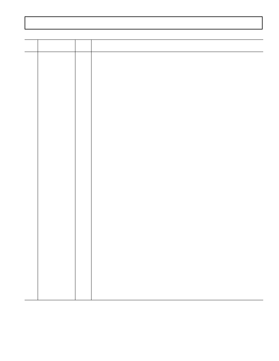
PIN FUNCTION DESCRIPTIONS (continued)
Pin
No.
Mnemonic
Type
Description
19
DVDD
P
Digital Power. Nominally at 5 V.
20
DGND
P
Digital Power Ground
21
DATA[8]
DO
When SER/
PAR is LOW, this output is used as the Bit 8 of the Parallel Port Data Output Bus.
or SDOUT
When SER/
PAR is HIGH, this output, part of the serial port, is used as a serial data output
synchronized to SCLK. Conversion results are stored in an on-chip register. The AD7677
provides the conversion result, MSB first, from its internal shift register. The DATA format is
determined by the logic level of OB/
2C. In serial mode, when EXT/INT is LOW, SDOUT
is valid on both edges of SCLK. In serial mode, when EXT/
INT is HIGH: If INVSCLK is
LOW, SDOUT is updated on SCLK rising edge and valid on the next falling edge. If INVSCLK
is HIGH, SDOUT is updated on SCLK falling edge and valid on the next rising edge.
22
DATA[9]
DI/O
When SER/
PAR is LOW, this output is used as the Bit 9 of the Parallel Port Data Output Bus.
or SCLK
When SER/
PAR is HIGH, this pin, part of the serial port, is used as a serial data clock input
or output, dependent upon the logic state of the EXT/
INT pin. The active edge where the
data SDOUT is updated depends upon the logic state of the INVSCLK pin.
23
DATA[10]
DO
When SER/
PAR is LOW, this output is used as the Bit 10 of the Parallel Port Data Output Bus.
or SYNC
When SER/
PAR is HIGH, this output, part of the serial port, is used as a digital output frame
synchronization for use with the internal data clock (EXT/
INT = Logic LOW). When a read
sequence is initiated and INVSYNC is LOW, SYNC is driven HIGH and remains HIGH
while SDOUT output is valid. When a read sequence is initiated and INVSYNC is HIGH,
SYNC is driven LOW and remains LOW while SDOUT output is valid.
24
DATA[11]
DO
When SER/
PAR is LOW, this output is used as the Bit 11 of the Parallel Port Data Output Bus.
or RDERROR
When SER/
PAR is HIGH and EXT/INT is HIGH, this output, part of the serial port, is used
as an incomplete read error flag. In slave mode, when a data read is started and not complete
when the following conversion is complete, the current data is lost and RDERROR is pulsed high.
25–28
DATA[12:15]
DO
Bit 12 to Bit 15 of the Parallel Port Data Output Bus. These pins are always outputs regard-
less of the state of SER/
PAR.
29
BUSY
DO
Busy Output. Transitions HIGH when a conversion is started, and remains HIGH until the
conversion is complete and the data is latched into the on-chip shift register. The falling edge
of BUSY could be used as a data ready clock signal.
30
DGND
P
Must be tied to digital ground.
31
RD
DI
Read Data. When
CS and RD are both LOW, the interface parallel or serial output bus is enabled.
32
CS
DI
Chip Select. When
CS and RD are both LOW, the interface parallel or serial output bus is
enabled.
CS is also used to gate the external serial clock.
33
RESET
DI
Reset Input. When set to a logic HIGH, reset the AD7677. Current conversion if any is aborted.
34
PD
DI
Power-Down Input. When set to a logic HIGH, power consumption is reduced and conver-
sions are inhibited after the current one is completed.
35
CNVST
DI
Start Conversion. A falling edge on
CNVST puts the internal sample/hold into the hold state and
initiates a conversion. In impulse mode (IMPULSE HIGH and WARP LOW), if
CNVST is
held low when the acquisition phase
(t
8) is complete, the internal sample/hold is put into the
hold state and a conversion is immediately started.
36
AGND
P
Must be Tied to Analog Ground.
37
REF
AI
Reference Input Voltage
38
REFGND
AI
Reference Input Analog Ground
39
IN–
AI
Differential Negative Analog Input
43
IN+
AI
Differential Positive Analog Input
NOTES
AI = Analog Input
DI = Digital Input
DI/O = Bidirectional Digital
DO = Digital Output
P = Power
相关PDF资料 |
PDF描述 |
|---|---|
| EVAL-AD7671CBZ | BOARD EVALUATION FOR AD7671 |
| 94SVP337X0016F12 | CAP ALUM 330UF 16V 20% SMD |
| EVAL-AD7654CBZ | BOARD EVALUATION FOR AD7654 |
| STD17W-P | WIRE & CABLE MARKERS |
| EVAL-AD7653CBZ | BOARD EVALUATION FOR AD7653 |
相关代理商/技术参数 |
参数描述 |
|---|---|
| EVAL-AD7677EDZ | 功能描述:BOARD EVAL FOR AD7677 RoHS:是 类别:编程器,开发系统 >> 评估板 - 模数转换器 (ADC) 系列:* 产品培训模块:Obsolescence Mitigation Program 标准包装:1 系列:- ADC 的数量:1 位数:12 采样率(每秒):94.4k 数据接口:USB 输入范围:±VREF/2 在以下条件下的电源(标准):- 工作温度:-40°C ~ 85°C 已用 IC / 零件:MAX11645 已供物品:板,软件 |
| EVAL-AD7678CB | 功能描述:BOARD EVALUATION FOR AD7678 RoHS:否 类别:编程器,开发系统 >> 评估板 - 模数转换器 (ADC) 系列:PulSAR® 产品培训模块:Obsolescence Mitigation Program 标准包装:1 系列:- ADC 的数量:1 位数:12 采样率(每秒):94.4k 数据接口:USB 输入范围:±VREF/2 在以下条件下的电源(标准):- 工作温度:-40°C ~ 85°C 已用 IC / 零件:MAX11645 已供物品:板,软件 |
| EVAL-AD7678CBZ | 功能描述:BOARD EVAL FOR AD7678 RoHS:是 类别:编程器,开发系统 >> 评估板 - 模数转换器 (ADC) 系列:PulSAR® 产品培训模块:Obsolescence Mitigation Program 标准包装:1 系列:- ADC 的数量:1 位数:12 采样率(每秒):94.4k 数据接口:USB 输入范围:±VREF/2 在以下条件下的电源(标准):- 工作温度:-40°C ~ 85°C 已用 IC / 零件:MAX11645 已供物品:板,软件 |
| EVAL-AD7678EDZ | 功能描述:BOARD EVAL FOR AD7678 RoHS:是 类别:编程器,开发系统 >> 评估板 - 模数转换器 (ADC) 系列:PulSAR® 产品培训模块:Obsolescence Mitigation Program 标准包装:1 系列:- ADC 的数量:1 位数:12 采样率(每秒):94.4k 数据接口:USB 输入范围:±VREF/2 在以下条件下的电源(标准):- 工作温度:-40°C ~ 85°C 已用 IC / 零件:MAX11645 已供物品:板,软件 |
| EVAL-AD7679CB | 制造商:Rochester Electronics LLC 功能描述:AD7679 EVAL BOARD 18BIT 570KSPS ADC - Bulk 制造商:Analog Devices 功能描述:AD7679 EVAL BOARD 18BIT 570KSPS ADC |
发布紧急采购,3分钟左右您将得到回复。