- 您现在的位置:买卖IC网 > PDF目录17047 > EVAL-AD7780EBZ (Analog Devices Inc)BOARD EVAL FOR AD7780 PDF资料下载
参数资料
| 型号: | EVAL-AD7780EBZ |
| 厂商: | Analog Devices Inc |
| 文件页数: | 6/16页 |
| 文件大小: | 0K |
| 描述: | BOARD EVAL FOR AD7780 |
| 标准包装: | 1 |
| ADC 的数量: | 1 |
| 位数: | 24 |
| 采样率(每秒): | 16.7 |
| 数据接口: | SPI? |
| 输入范围: | ±5 V |
| 工作温度: | -40°C ~ 105°C |
| 已用 IC / 零件: | AD7780 |
| 已供物品: | 板 |
AD7780
Rev. A | Page 14 of 16
APPLICATIONS INFORMATION
The AD7780 provides a low cost, high resolution analog-to-digital
function. Because the analog-to-digital function is provided by a
Σ-Δ architecture, the parts are more immune to noisy environ-
ments, making them ideal for use in sensor measurement and
industrial and process control applications.
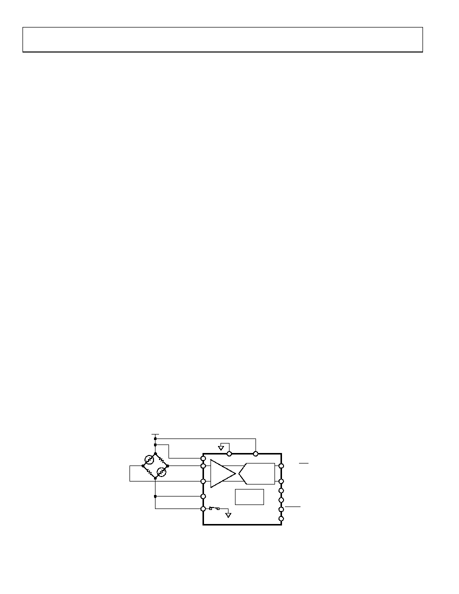
WEIGH SCALES
Figure 23 shows the AD7780 being used in a weigh scale
application. The load cell is arranged in a bridge network and
gives a differential output voltage between its OUT+ and OUT
terminals. Assuming a 5 V excitation voltage, the full-scale
output range from the transducer is 10 mV when the sensitivity
is 2 mV/V. The excitation voltage for the bridge can be used to
directly provide the reference for the ADC because the refer-
ence input range includes the supply voltage.
A second advantage of using the AD7780 in transducer-based
applications is that the bridge power-down switch (BPDSW)
can be fully utilized in low power applications. The bridge power-
down switch is connected in series with the low side of the bridge.
In normal operation, the switch is closed and measurements
can be taken. In applications where power is of concern, the
AD7780 can be placed in power-down mode, significantly
reducing the power consumed in the application. In addition,
the bridge power-down switch is opened while in power-down
mode, thus avoiding unnecessary power consumption by the
front-end transducer. When the part is taken out of power-down
mode and the bridge power-down switch is closed, the user should
ensure that the front-end circuitry is fully settled before attempting
a read from the AD7780.
The load cell has an offset or tare associated with it. This tare is
the main component of the system offset (load cell + ADC) and is
similar in magnitude to the full-scale signal from the load cell.
For this reason, calibrating the offset and gain of the AD7780 alone
is not sufficient for optimum accuracy; a system calibration that
calibrates the offset and gain of the ADC, plus the load cell, is
required. A microprocessor can be used to perform the calibra-
tions. The offset (the conversion result from the AD7780 when
no load is applied to the load cell) and the full-scale error (the
conversion result from the ADC when the maximum load is
applied to the load cell) must be determined. Subsequent conver-
sions from the AD7780 are then corrected, using the offset and
gain coefficients that were calculated from these calibrations.
PERFORMANCE IN A WEIGH SCALE SYSTEM
If the load cell has a sensitivity of 2 mV/V and a 5 V excitation
voltage is used, the full-scale signal from the load cell is 10 mV.
When the AD7780 operates with a 10 Hz output data rate and
the gain is set to 128, the device has a p-p resolution of 18.2 bits
when the reference is equal to 5 V. Postprocessing the data from
the AD7780 using a microprocessor increases the p-p resolution.
For example, an average by 4 in the microprocessor increases
the accuracy by 2 bits. The noise-free counts is equal to the
following:
Noise-Free Counts = (2Effective Bits)(FSLC/FSADC)
where:
Effective Bits = 18.2 bits + 2 bits (due to post-processing in the
microprocessor).
FSLC is the full-scale signal from the load cell (10 mV).
FSADC is the full-scale input range when gain = 128 and VREF = 5 V
(78 mV).
The noise-free counts are equal to the following:
(218.2 + 2)(10 mV/78 mV) = 154,422
This example shows that with a 5 V supply, 154,422 noise-free
counts can be achieved with the AD7780.
EMI RECOMMENDATIONS
For simplicity, the EMI filters are not included in Figure 23.
However, an R-C antialiasing filter should be included on each
analog input. This filter is needed because the on-chip digital
filter does not provide any rejection around the master clock or
multiples of the master clock. Suitable values are a 1 kΩ resistor
in series with each analog input, a 0.1 μF capacitor from AIN(+)
to AIN(), and 0.01 μF capacitors from AIN(+)/AIN() to GND.
G = 1
OR 128
24-BIT Σ-Δ
ADC
DOUT/RDY
GND
AVDD
AIN(+)
REFIN(+)
AIN(–)
SCLK
DVDD
FILTER
GAIN
INTERNAL
CLOCK
AD7780
PDRST
BPDSW
REFIN(–)
VDD
OUT–
IN+
IN–
OUT+
0
79
45
-02
2
Figure 23. Weigh Scales Using the AD7780
相关PDF资料 |
PDF描述 |
|---|---|
| ECC31DJXN-S1136 | CONN EDGECARD 62PS .100 PRESSFIT |
| ECC19DRAN | CONN EDGECARD 38POS R/A .100 SLD |
| SLP681M200C7P3 | CAP ALUM 680UF 200V 20% SNAP |
| EVAL-AD5453EBZ | BOARD EVALUATION FOR AD5453 |
| 380LX472M050K012 | CAP ALUM 4700UF 50V 20% SNAP |
相关代理商/技术参数 |
参数描述 |
|---|---|
| EVAL-AD7781EBZ | 功能描述:BOARD EVAL FOR AD7781 RoHS:是 类别:编程器,开发系统 >> 评估板 - 模数转换器 (ADC) 系列:- 产品培训模块:Obsolescence Mitigation Program 标准包装:1 系列:- ADC 的数量:1 位数:12 采样率(每秒):94.4k 数据接口:USB 输入范围:±VREF/2 在以下条件下的电源(标准):- 工作温度:-40°C ~ 85°C 已用 IC / 零件:MAX11645 已供物品:板,软件 |
| EVAL-AD7782EB | 制造商:Analog Devices 功能描述:READ ONLY, PIN CONFIGURED 24BIT SEGMA-DELTA ADC - Bulk |
| EVAL-AD7783EB | 制造商:Analog Devices 功能描述:EVALUATION BOARD I.C. - Bulk |
| EVAL-AD7783EBZ | 功能描述:BOARD EVAL FOR AD7783 RoHS:是 类别:编程器,开发系统 >> 评估板 - 模数转换器 (ADC) 系列:- 产品培训模块:Obsolescence Mitigation Program 标准包装:1 系列:- ADC 的数量:1 位数:12 采样率(每秒):94.4k 数据接口:USB 输入范围:±VREF/2 在以下条件下的电源(标准):- 工作温度:-40°C ~ 85°C 已用 IC / 零件:MAX11645 已供物品:板,软件 |
| EVAL-AD7785EBZ | 功能描述:BOARD EVALUATION FOR AD7785 RoHS:是 类别:编程器,开发系统 >> 评估板 - 模数转换器 (ADC) 系列:- 产品培训模块:Obsolescence Mitigation Program 标准包装:1 系列:- ADC 的数量:1 位数:12 采样率(每秒):94.4k 数据接口:USB 输入范围:±VREF/2 在以下条件下的电源(标准):- 工作温度:-40°C ~ 85°C 已用 IC / 零件:MAX11645 已供物品:板,软件 |
发布紧急采购,3分钟左右您将得到回复。