- 您现在的位置:买卖IC网 > PDF目录17060 > EVAL-AD7793EBZ (Analog Devices Inc)BOARD EVALUATION FOR AD7793 PDF资料下载
参数资料
| 型号: | EVAL-AD7793EBZ |
| 厂商: | Analog Devices Inc |
| 文件页数: | 9/33页 |
| 文件大小: | 0K |
| 描述: | BOARD EVALUATION FOR AD7793 |
| 标准包装: | 1 |
| ADC 的数量: | 1 |
| 位数: | 24 |
| 采样率(每秒): | 470 |
| 数据接口: | 串行 |
| 输入范围: | 0 ~ 5 V |
| 在以下条件下的电源(标准): | 2.5mW @ 470SPS |
| 工作温度: | -40°C ~ 105°C |
| 已用 IC / 零件: | AD7793 |
| 已供物品: | 板,缆线,CD |
| 相关产品: | AD7793BRU-ND - IC ADC 24BIT 3CH LP 16-TSSOP AD7793BRUZ-REEL-ND - IC ADC 24BIT 3CH LP 16-TSSOP AD7793BRUZ-ND - IC ADC 24BIT SIG-DEL 3CH 16TSSOP |
第1页第2页第3页第4页第5页第6页第7页第8页当前第9页第10页第11页第12页第13页第14页第15页第16页第17页第18页第19页第20页第21页第22页第23页第24页第25页第26页第27页第28页第29页第30页第31页第32页第33页
AD7792/AD7793
Rev. B | Page 16 of 32
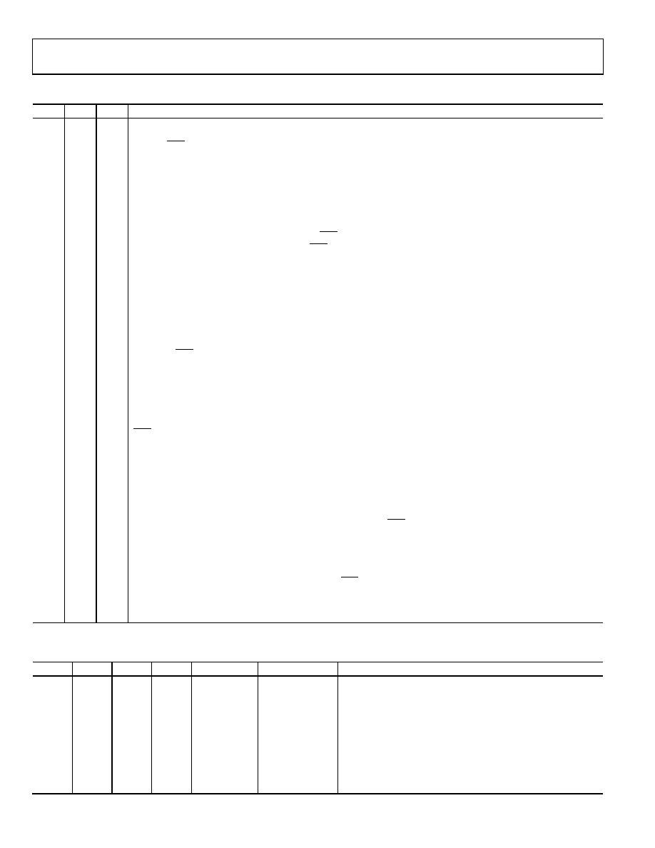
Table 15. Operating Modes
MD2
MD1
MD0
Mode
0
Continuous Conversion Mode (Default).
In continuous conversion mode, the ADC continuously performs conversions and places the result in the data
register. RDY goes low when a conversion is complete. The user can read these conversions by placing the device in
continuous read mode, whereby the conversions are automatically placed on the DOUT line when SCLK pulses are
applied. Alternatively, the user can instruct the ADC to output the conversion by writing to the communications
register. After power-on, a channel change, or a write to the mode, configuration, or IO registers, the first conversion
is available after a period of 2/fADC. Subsequent conversions are available at a frequency of fADC.
0
1
Single Conversion Mode.
When single conversion mode is selected, the ADC powers up and performs a single conversion. The oscillator
requires 1 ms to power up and settle. The ADC then performs the conversion, which takes a time of 2/fADC. The
conversion result is placed in the data register, RDY goes low, and the ADC returns to power-down mode. The
conversion remains in the data register, and RDY remains active low until the data is read or another conversion is
performed.
0
1
0
Idle Mode.
In idle mode, the ADC filter and modulator are held in a reset state, although the modulator clocks are still provided.
0
1
Power-Down Mode.
In power-down mode, all the AD7792/AD7793 circuitry is powered down, including the current sources, burnout
currents, bias voltage generator, and CLKOUT circuitry.
1
0
Internal Zero-Scale Calibration.
An internal short is automatically connected to the enabled channel. A calibration takes 2 conversion cycles to
complete. RDY goes high when the calibration is initiated and returns low when the calibration is complete. The
ADC is placed in idle mode following a calibration. The measured offset coefficient is placed in the offset register of
the selected channel.
1
0
1
Internal Full-Scale Calibration.
A full-scale input voltage is automatically connected to the selected analog input for this calibration.
When the gain equals 1, a calibration takes 2 conversion cycles to complete. For higher gains, 4 conversion cycles
are required to perform the full-scale calibration.
RDY goes high when the calibration is initiated and returns low when the calibration is complete. The ADC is placed
in idle mode following a calibration. The measured full-scale coefficient is placed in the full-scale register of the
selected channel.
Internal full-scale calibrations cannot be performed when the gain equals 128. With this gain setting, a system full-
scale calibration can be performed.
A full-scale calibration is required each time the gain of a channel is changed to minimize the full-scale error.
1
0
System Zero-Scale Calibration.
User should connect the system zero-scale input to the channel input pins as selected by the CH2 to CH0 bits. A
system offset calibration takes 2 conversion cycles to complete. RDY goes high when the calibration is initiated and
returns low when the calibration is complete. The ADC is placed in idle mode following a calibration. The measured
offset coefficient is placed in the offset register of the selected channel.
1
System Full-Scale Calibration.
User should connect the system full-scale input to the channel input pins as selected by the CH2 to CH0 bits.
A calibration takes 2 conversion cycles to complete. RDY goes high when the calibration is initiated and returns low
when the calibration is complete. The ADC is placed in idle mode following a calibration. The measured full-scale
coefficient is placed in the full-scale register of the selected channel.
A full-scale calibration is required each time the gain of a channel is changed.
Table 16. Update Rates Available
FS3
FS2
FS1
FS0
fADC (Hz)
tSETTLE (ms)
Rejection @ 50 Hz/60 Hz (Internal Clock)
0
x
0
1
470
4
0
1
0
242
8
0
1
123
16
0
1
0
62
32
0
1
0
1
50
40
0
1
0
39
48
0
1
33.2
60
1
0
19.6
101
90 dB (60 Hz only)
相关PDF资料 |
PDF描述 |
|---|---|
| RCM15DCBD-S189 | CONN EDGECARD 30POS R/A .156 SLD |
| 0982660775 | CBL 9POS 0.5MM JMPR TYPE A 5" |
| EVAL-AD7734EBZ | BOARD EVALUATION FOR AD7734 |
| SK471M100ST | CAP ALUM 470UF 100V 20% RADIAL |
| 0982660774 | CBL 9POS 0.5MM JMPR TYPE D 5" |
相关代理商/技术参数 |
参数描述 |
|---|---|
| EVAL-AD7793EBZ | 制造商:Analog Devices 功能描述:EVAL BOARD, AD7793 3CH 24BIT ADC |
| EVAL-AD7793EBZ1 | 制造商:AD 制造商全称:Analog Devices 功能描述:3-Channel, Low Noise, Low Power, 16-/24-Bit ?£-?? ADC with On-Chip In-Amp and Reference |
| EVAL-AD7794EB | 制造商:Analog Devices 功能描述:EVALUATION BOARD I.C. - Bulk |
| EVAL-AD7794EBZ | 功能描述:BOARD EVALUATION FOR AD7794 RoHS:是 类别:编程器,开发系统 >> 评估板 - 模数转换器 (ADC) 系列:- 产品培训模块:Obsolescence Mitigation Program 标准包装:1 系列:- ADC 的数量:1 位数:12 采样率(每秒):94.4k 数据接口:USB 输入范围:±VREF/2 在以下条件下的电源(标准):- 工作温度:-40°C ~ 85°C 已用 IC / 零件:MAX11645 已供物品:板,软件 |
| EVAL-AD7795 | 制造商:AD 制造商全称:Analog Devices 功能描述:Evaluation Board for the AD7795 16-Bit, Low Power Sigma-Delta ADC (6 Channels) |
发布紧急采购,3分钟左右您将得到回复。