- 您现在的位置:买卖IC网 > PDF目录17055 > EVAL-AD7797EBZ (Analog Devices Inc)BOARD EVALUATION FOR AD7797 PDF资料下载
参数资料
| 型号: | EVAL-AD7797EBZ |
| 厂商: | Analog Devices Inc |
| 文件页数: | 3/24页 |
| 文件大小: | 0K |
| 描述: | BOARD EVALUATION FOR AD7797 |
| 标准包装: | 1 |
| ADC 的数量: | 1 |
| 位数: | 24 |
| 采样率(每秒): | 123 |
| 数据接口: | 串行 |
| 输入范围: | ±VREF/128 |
| 在以下条件下的电源(标准): | 1.6mW @ 123SPS |
| 工作温度: | -40°C ~ 85°C |
| 已用 IC / 零件: | AD7797 |
| 已供物品: | 板,CD |
| 相关产品: | AD7797BRUZ-REEL-ND - IC ADC 24BIT SIG-DEL 1CH 16TSSOP AD7797BRUZ-ND - IC ADC 24BIT SIG-DEL 1CH 16TSSOP |

AD7796/AD7797
Rev. A | Page 11 of 24
ON-CHIP REGISTERS
The ADC is controlled and configured via a number of on-chip
registers, which are described on the following pages. In the
following descriptions, set implies a Logic 1 State and cleared
implies a Logic 0 State, unless otherwise stated.
COMMUNICATION REGISTER
RS2, RS1, RS0 = 0, 0, 0
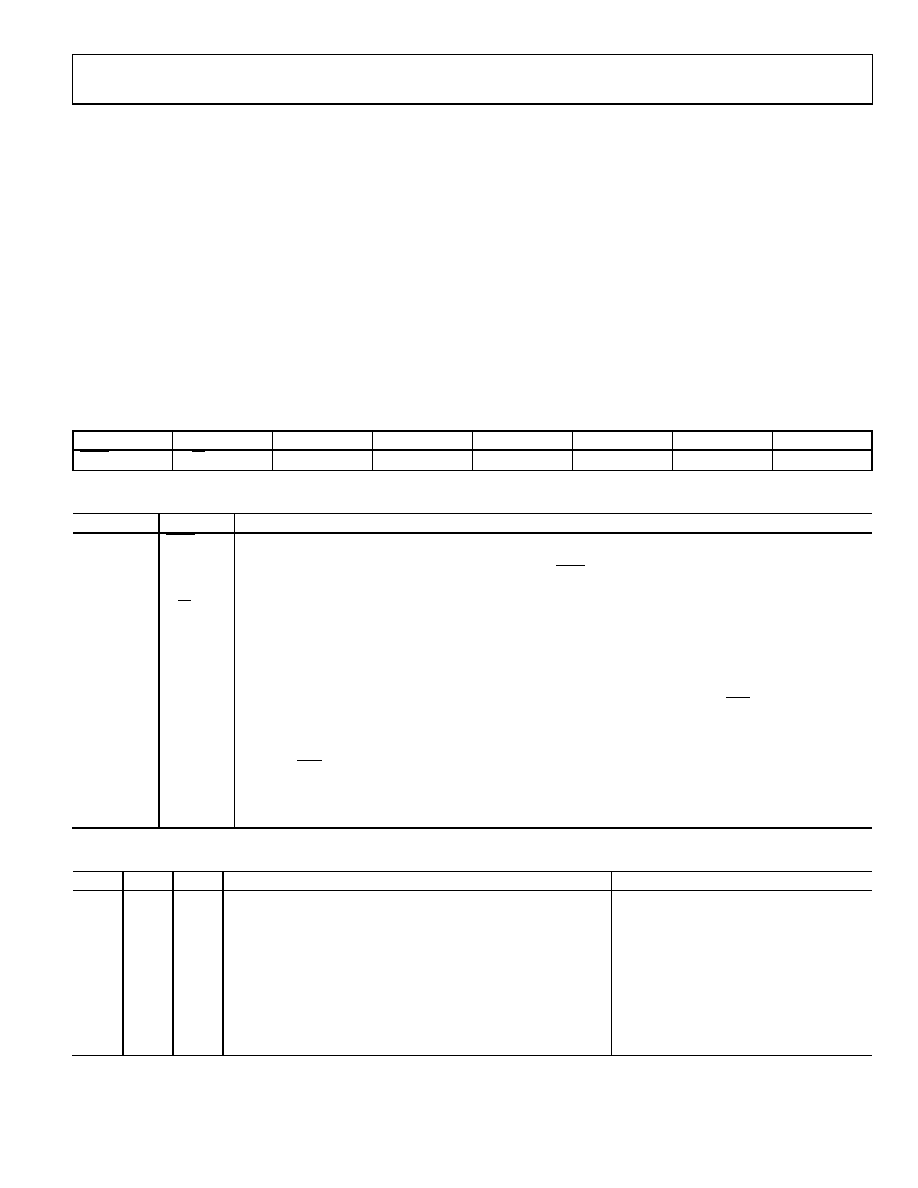
The communication register is an 8-bit write-only register. All
communication to the part must start with a write operation to
this register. The data written to the communication register
determines whether the next operation is a read or write opera-
tion, and selects the register where this operation takes place.
Once the subsequent read or write operation to the selected
register is complete, the interface returns to where it expects a
write operation to the communication register (this is the
default state of the interface). On power-up or after a reset, the
ADC is in this default state waiting for a write operation to the
communication register. In situations where the interface
sequence is lost, a write operation of at least 32 serial clock
cycles with DIN high returns the ADC to this default state by
resetting the entire part. Table 9 outlines the bit designations for
the communication register. CR0 through CR7 indicate the bit
location, with CR denoting that the bits are in the communication
register. CR7 denotes the first bit of the data stream. The number
in brackets indicates the power-on/reset default status of that bit.
MSB
LSB
CR7
CR6
CR5
CR4
CR3
CR2
CR1
CR0
WEN(0)
R/W(0)
RS2(0)
RS1(0)
RS0(0)
CREAD(0)
0(0)
Table 9. Communication Register Bit Designations
Bit Location
Bit Name
Description
CR7
WEN
Write Enable Bit. A 0 must be written to this bit first to ensure that a write to the communication register
occurs. If a 1 is the first bit written, the part does not clock onto subsequent bits in the register; it stays at this
bit location until a 0 is written. Once a 0 is written to the WEN bit, the next seven bits are loaded to the
communication register.
CR6
R/W
A 0 in this bit location indicates that the next operation is a write to a specified register. A 1 in this position
indicates that the next operation is a read from the designated register.
CR5 to CR3
RS2 to RS0
Register Address Bits. These address bits determine which ADC registers are being selected during this serial
interface communication. See Table 10.
CR2
CREAD
Continuous Read of the Data Register. When this bit is set to 1 (and the data register is selected), the serial
interface is configured to continuously read the data register. For example, the contents of the data register are
automatically placed on the DOUT pin when the SCLK pulses are applied and after the RDY pin goes low. This
indicates that a conversion is complete. The communication register does not have to be written to for data reads.
To enable continuous read mode, the instruction 01011100 must be written to the communication register.
To exit the continuous read mode, the instruction 01011000 must be written to the communication register
while the RDY pin is low. While in continuous read mode, the ADC monitors activity on the DIN line so it can
receive the instruction to exit continuous read mode. Additionally, a reset occurs if 32 consecutive 1s are seen
on DIN. Therefore, DIN should be held low in continuous read mode until an instruction is written to the device.
CR1 to CR0
0
These bits must be programmed to Logic 0 for correct operation.
Table 10. Register Selection
RS2
RS1
RS0
Register
Register Size
0
Communication Register During a Write Operation
8 bits
0
Status Register During a Read Operation
8 bits
0
1
Mode Register
16 bits
0
1
0
Configuration Register
16 bits
0
1
Data Register
16 bits (AD7796), 24 bits (AD7797)
1
0
ID Register
8 bits
1
0
1
Reserved
8 bits
1
0
Offset Register
16 bits (AD7796), 24 bits (AD7797)
1
Full-Scale Register
16 bits (AD7796), 24 bits (AD7797)
相关PDF资料 |
PDF描述 |
|---|---|
| GCA18DTAD | CONN EDGECARD 36POS R/A .125 SLD |
| MIC2018YML TR | IC DISTRIBUTION SW ADJ 6-MLF |
| EMC12DRES | CONN EDGECARD 24POS .100 EXTEND |
| MIC2563A-1YSM | IC CTRLR PCMCIA CARDBS DL 28SSOP |
| EYM08DTKT | CONN EDGECARD 16POS DIP .156 SLD |
相关代理商/技术参数 |
参数描述 |
|---|---|
| EVAL-AD7798EB | 制造商:Analog Devices 功能描述:EVAL BD LOW PWR, 16BIT BFFRED SIGMA-DELTA ADC - Bulk |
| EVAL-AD7798EBZ | 功能描述:BOARD EVAL FOR AD7798 RoHS:是 类别:编程器,开发系统 >> 评估板 - 模数转换器 (ADC) 系列:- 产品培训模块:Obsolescence Mitigation Program 标准包装:1 系列:- ADC 的数量:1 位数:12 采样率(每秒):94.4k 数据接口:USB 输入范围:±VREF/2 在以下条件下的电源(标准):- 工作温度:-40°C ~ 85°C 已用 IC / 零件:MAX11645 已供物品:板,软件 |
| EVAL-AD7799EBZ | 功能描述:BOARD EVALUATION FOR AD7799 RoHS:是 类别:编程器,开发系统 >> 评估板 - 模数转换器 (ADC) 系列:- 产品培训模块:Obsolescence Mitigation Program 标准包装:1 系列:- ADC 的数量:1 位数:12 采样率(每秒):94.4k 数据接口:USB 输入范围:±VREF/2 在以下条件下的电源(标准):- 工作温度:-40°C ~ 85°C 已用 IC / 零件:MAX11645 已供物品:板,软件 |
| EVAL-AD7816/7/8EB | 制造商:Analog Devices 功能描述:EVALUATION BOARD I.C. - Bulk |
| EVAL-AD7816EB | 制造商:AD 制造商全称:Analog Devices 功能描述:Single- and 4-Channel, 9 us, 10-Bit ADCs with On-Chip Temperature Sensor |
发布紧急采购,3分钟左右您将得到回复。