- 您现在的位置:买卖IC网 > PDF目录17070 > EVAL-AD7839EBZ (Analog Devices Inc)BOARD EVAL FOR AD7839 PDF资料下载
参数资料
| 型号: | EVAL-AD7839EBZ |
| 厂商: | Analog Devices Inc |
| 文件页数: | 12/12页 |
| 文件大小: | 0K |
| 描述: | BOARD EVAL FOR AD7839 |
| 产品培训模块: | DAC Architectures |
| 标准包装: | 1 |
| DAC 的数量: | 8 |
| 位数: | 13 |
| 采样率(每秒): | 33k |
| 数据接口: | 并联 |
| 设置时间: | 30µs |
| DAC 型: | 电压 |
| 工作温度: | -40°C ~ 85°C |
| 已供物品: | 板,缆线,CD |
| 已用 IC / 零件: | AD7839 |
| 相关产品: | AD7839ASZ-REEL-ND - IC DAC 13BIT OCT VOLT OUT 44MQFP AD7839ASZ-ND - IC DAC 13BIT OCTAL V-OUT 44-MQFP |
AD7839
–9–
REV. 0
Power-On with
CLR Low
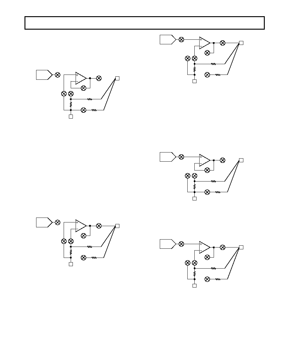
The output stage of the AD7839 has been designed to allow
output stability during power-on. If
CLR is kept low during
power-on, then just after power is applied to the AD7839, the
situation is as depicted in Figure 14. G1, G4 and G6 are open
while G2, G3 and G5 are closed.
G1
G2
G4
G3
G6
G5
DUTGND
VOUT
R
14k
DAC
Figure 14. Output Stage with VDD < 7 V or VSS > –3 V;
CLR Low
VOUT is kept within a few hundred millivolts of DUTGND via
G5 and a 14 k
resistor. This thin-film resistor is connected in
parallel with the gain resistors of the output amplifier. The
output amplifier is connected as a unity gain buffer via G3, and
the DUTGND voltage is applied to the buffer input via G2. The
amplifier’s output is thus at the same voltage as the DUTGND
pin. The output stage remains configured as in Figure 14 until
the voltage at VDD exceeds 7 V and VSS is more negative than
–3 V. By now the output amplifier has enough headroom to
handle signals at its input and has also had time to settle. The
internal power-on circuitry opens G3 and G5 and closes G4 and
G6. This situation is shown in Figure 15. Now the output ampli-
fier is configured in its noise gain configuration via G4 and G6.
The DUTGND voltage is still connected to the noninverting
input via G2 and this voltage appears at VOUT.
G1
G2
G4
G3
G6
G5
DUTGND
VOUT
R
14k
DAC
Figure 15. Output Stage with VDD > 7 V and VSS < –3 V;
CLR Low
VOUT has been disconnected from the DUTGND pin by the
opening of G5, but will track the voltage present at DUTGND
via the configuration shown in Figure 15.
When
CLR is taken back high, the output stage is configured as
shown in Figure 16. The internal control logic closes G1 and
opens G2. The output amplifier is connected in a noninverting
gain-of-two configuration. The voltage that appears on the VOUT
pins is determined by the data present in the DAC registers.
G1
G2
G4
G3
G6
G5
DUTGND
VOUT
R
14k
DAC
Figure 16. Output Stage After
CLR Is Taken High
Power-On with
CLR High
If
CLR is high on the application of power to the device, the
output stages of the AD7839 are configured as in Figure 17
while VDD is less than 7 V and VSS is more positive than –3 V.
G1 is closed and G2 is open, thereby connecting the output of the
DAC to the input of its output amplifier. G3 and G5 are closed
while G4 and G6 are open, thus connecting the output amplifier as
a unity gain buffer. VOUT is connected to DUTGND via G5
through a 14 k
resistor until V
DD exceeds 7 V and VSS is more
negative than –3 V.
G1
G2
G4
G3
G6
G5
DUTGND
VOUT
R
14k
DAC
Figure 17. Output Stage Powering Up with
CLR High
While VDD < 7 V or VSS > –3 V
When the difference between the supply voltages reaches +10 V,
the internal power-on circuitry opens G3 and G5 and closes G4
and G6 configuring the output stage as shown in Figure 18.
G1
G2
G4
G3
G6
G5
DUTGND
VOUT
R
14k
DAC
Figure 18. Output Stage Powering Up with
CLR High;
VDD > 7 V and VSS < –3 V
相关PDF资料 |
PDF描述 |
|---|---|
| NRS6010T4R7MMGF | INDUCTOR POWER 4.7UH 1.4A SMD |
| AD7940-DBRD | BOARD EVAL FOR AD7940 STAMP SPI |
| EVAL-AD5663REBZ | BOARD EVAL FOR AD5663 |
| NRS6010T3R3MMGF | INDUCTOR POWER 3.3UH 1.5A SMD |
| EVAL-AD5390EBZ | BOARD EVALUATION FOR AD5390 |
相关代理商/技术参数 |
参数描述 |
|---|---|
| EVAL-AD7841EB | 制造商:Rochester Electronics LLC 功能描述: 制造商:Analog Devices 功能描述: |
| EVAL-AD7841EBZ | 功能描述:BOARD EVAL FOR AD7841 RoHS:是 类别:编程器,开发系统 >> 评估板 - 数模转换器 (DAC) 系列:- 产品培训模块:Lead (SnPb) Finish for COTS Obsolescence Mitigation Program 标准包装:1 系列:- DAC 的数量:4 位数:12 采样率(每秒):- 数据接口:串行,SPI? 设置时间:3µs DAC 型:电流/电压 工作温度:-40°C ~ 85°C 已供物品:板 已用 IC / 零件:MAX5581 |
| EVAL-AD7843CB | 制造商:AD 制造商全称:Analog Devices 功能描述:Touch Screen Digitizer |
| EVAL-AD7843CB3 | 制造商:AD 制造商全称:Analog Devices 功能描述:Touch Screen Digitizer |
| EVAL-AD7843EBZ | 功能描述:BOARD EVAL FOR AD7843 RoHS:是 类别:编程器,开发系统 >> 评估板 - 模数转换器 (ADC) 系列:- 产品培训模块:Obsolescence Mitigation Program 标准包装:1 系列:- ADC 的数量:1 位数:12 采样率(每秒):94.4k 数据接口:USB 输入范围:±VREF/2 在以下条件下的电源(标准):- 工作温度:-40°C ~ 85°C 已用 IC / 零件:MAX11645 已供物品:板,软件 |
发布紧急采购,3分钟左右您将得到回复。