- 您现在的位置:买卖IC网 > PDF目录17051 > EVAL-AD7899CBZ (Analog Devices Inc)BOARD EVAL FOR AD7899 PDF资料下载
参数资料
| 型号: | EVAL-AD7899CBZ |
| 厂商: | Analog Devices Inc |
| 文件页数: | 6/16页 |
| 文件大小: | 0K |
| 描述: | BOARD EVAL FOR AD7899 |
| 标准包装: | 1 |
| ADC 的数量: | 1 |
| 位数: | 14 |
| 采样率(每秒): | 400k |
| 数据接口: | 并联 |
| 输入范围: | ±10 V |
| 在以下条件下的电源(标准): | 80mW @ 400kSPS |
| 工作温度: | -40°C ~ 85°C |
| 已用 IC / 零件: | AD7899 |
| 已供物品: | 板 |
| 相关产品: | AD7899ARZ-2-ND - IC ADC 14BIT 400KSPS 5V 28SOIC AD7899BRZ-3-ND - IC ADC 14BIT 400KSPS 5V 28SOIC AD7899BRZ-1-ND - IC ADC 14BIT 400KSPS 5V 28SOIC AD7899ARZ-3-ND - IC ADC 14BIT 400KSPS 5V 28SOIC AD7899ARZ-1-ND - IC ADC 14BIT 400KSPS 5V 28SOIC AD7899ARSZ-3-ND - IC ADC 14BIT 400KSPS 5V 28SSOP AD7899ARSZ-2-ND - IC ADC 14BIT 400KSPS 5V 28-SSOP AD7899ARSZ-1REEL7-ND - IC ADC 14BIT 400KSPS 5V 28SSOP AD7899ARZ-1REEL-ND - IC ADC 14BIT 400KSPS 5V 28SOIC AD7899ARSZ-3REEL-ND - IC ADC 14BIT 400KSPS 5V 28SSOP 更多... |
REV. A
AD7899
–14–
MICROPROCESSOR INTERFACING
The high-speed parallel interface of the AD7899 allows easy
interfacing to most DSPs and microprocessors. The AD7899
interface of the AD7899 consists of the data lines (DB0 to DB13),
CS, RD, and BUSY/EOC.
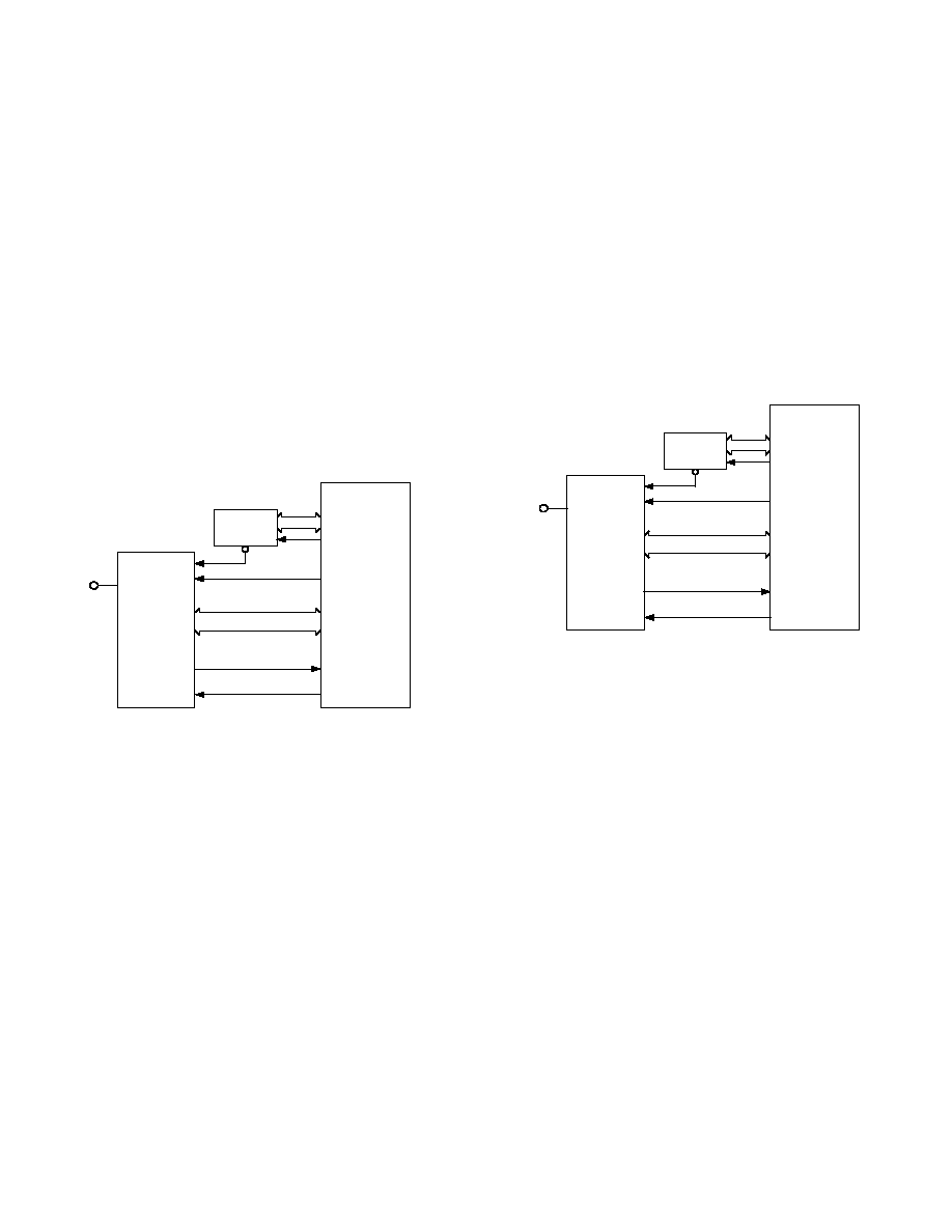
AD7899–ADSP-21xx Interface
Figure 14 shows an interface between the AD7899 and the
ADSP-21xx. The
CONVST signal can be generated by the
ADSP-21xx or from some other external source. Figure 14 shows
the
CS being generated by a combination of the DMS signal and
the address bus of the ADSP-21xx. In this way the AD7899 is
mapped into the data memory space of the ADSP-21xx.
The AD7899 BUSY/
EOC line provides an interrupt to the
ADSP-21xx when the conversion is complete. The conversion
result can then be read from the AD7899 using a read operation.
The AD7899 is read using the following instruction
MR0 = DM(ADC)
where MR0 is the ADSP-21xx MR0 register and ADC is the
AD7899 address.
CS
RD
CONVST
DB0–DB13
AD7899
VIN
DT1/F0
IRQn
D8–D21
A0–A13
ADSP-21xx
ADDRESS
DECODE
RD
DMS
BUSY/
EOC
Figure 14. AD7899–ADSP-21xx Interface
AD7899–TMS320C5x Interface
Figure 15 shows an interface between the AD7899 and the
TMS320C5x. As with the previous interfaces, conversion can be
initiated from the TMS320C5x or from an external source and
the processor is interrupted when the conversion sequence is
completed. The
CS signal to the AD7899 derived from the DS
signal and a decode of the address bus. This maps the AD7899
into external data memory. The
RD signal from the TMS320 is
used to enable the ADC data onto the data bus. The AD7899 has
a fast parallel bus so there are no wait state requirements. The
following instruction is used to read the conversion results from
the AD7899:
IN D,ADC
where D is Data Memory address and ADC is the AD7899
address.
CS
RD
BUSY/
EOC
CONVST
DB0–DB13
AD7899
VIN
PA0
INTn
D0–D13
DS
A0–A13
TMS320C5x
ADDRESS
DECODE
RD
Figure 15. AD7899–TMS320C5x Interface
相关PDF资料 |
PDF描述 |
|---|---|
| VI-BND-EY | CONVERTER MOD DC/DC 85V 50W |
| AT-S-26-8/8/W-25-R | MOD CORD STANDARD 8-8 WHITE 25' |
| EBC35DRYN | CONN EDGECARD 70POS DIP .100 SLD |
| EVAL-AD7327CBZ | BOARD EVALUATION FOR AD7327 |
| VI-BNB-EY | CONVERTER MOD DC/DC 95V 50W |
相关代理商/技术参数 |
参数描述 |
|---|---|
| EVAL-AD7910CB | 制造商:AD 制造商全称:Analog Devices 功能描述:250 kSPS, 10-/12-Bit ADCs in 6-Lead SC70 |
| EVAL-AD7910CBZ | 功能描述:BOARD EVALUATION FOR AD7910 RoHS:是 类别:编程器,开发系统 >> 评估板 - 模数转换器 (ADC) 系列:- 产品培训模块:Obsolescence Mitigation Program 标准包装:1 系列:- ADC 的数量:1 位数:12 采样率(每秒):94.4k 数据接口:USB 输入范围:±VREF/2 在以下条件下的电源(标准):- 工作温度:-40°C ~ 85°C 已用 IC / 零件:MAX11645 已供物品:板,软件 |
| EVAL-AD7912CB | 功能描述:BOARD EVALUATION FOR AD7912 RoHS:否 类别:编程器,开发系统 >> 评估板 - 模数转换器 (ADC) 系列:- 产品培训模块:Obsolescence Mitigation Program 标准包装:1 系列:- ADC 的数量:1 位数:12 采样率(每秒):94.4k 数据接口:USB 输入范围:±VREF/2 在以下条件下的电源(标准):- 工作温度:-40°C ~ 85°C 已用 IC / 零件:MAX11645 已供物品:板,软件 |
| EVAL-AD7912CBZ | 功能描述:BOARD EVALUATION FOR AD7912 RoHS:是 类别:编程器,开发系统 >> 评估板 - 模数转换器 (ADC) 系列:- 产品培训模块:Obsolescence Mitigation Program 标准包装:1 系列:- ADC 的数量:1 位数:12 采样率(每秒):94.4k 数据接口:USB 输入范围:±VREF/2 在以下条件下的电源(标准):- 工作温度:-40°C ~ 85°C 已用 IC / 零件:MAX11645 已供物品:板,软件 |
| EVAL-AD7920CB | 制造商:AD 制造商全称:Analog Devices 功能描述:250 kSPS, 10-/12-Bit ADCs in 6-Lead SC70 |
发布紧急采购,3分钟左右您将得到回复。