- 您现在的位置:买卖IC网 > PDF目录17036 > EVAL-AD7982SDZ (Analog Devices Inc)BOARD EVAL FOR AD7982 PDF资料下载
参数资料
| 型号: | EVAL-AD7982SDZ |
| 厂商: | Analog Devices Inc |
| 文件页数: | 16/24页 |
| 文件大小: | 0K |
| 描述: | BOARD EVAL FOR AD7982 |
| 标准包装: | 1 |
| 系列: | PulSAR® |
| ADC 的数量: | 1 |
| 位数: | 18 |
| 采样率(每秒): | 1M |
| 数据接口: | DSP,MICROWIRE?,QSPI?,串行,SPI? |
| 输入范围: | ±VREF |
| 在以下条件下的电源(标准): | 7mW @ 1MSPS |
| 工作温度: | -40°C ~ 85°C |
| 已用 IC / 零件: | AD7982 |
| 已供物品: | 板 |
Data Sheet
AD7982
Rev. B | Page 23 of 24
APPLICATION HINTS
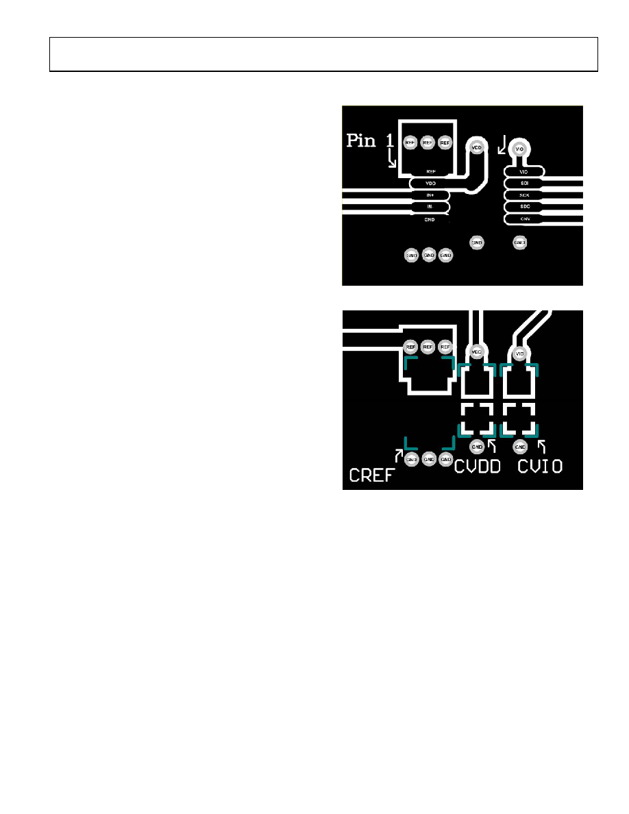
LAYOUT
The printed circuit board that houses the AD7982 should be
designed so that the analog and digital sections are separated
and confined to certain areas of the board. The pinout of the
AD7982, with its analog signals on the left side and its digital
signals on the right side, eases this task.
Avoid running digital lines under the device because these
couple noise onto the die, unless a ground plane under the
AD7982 is used as a shield. Fast switching signals, such as CNV
or clocks, should not run near analog signal paths. Crossover of
digital and analog signals should be avoided.
At least one ground plane should be used. It can be common or
split between the digital and analog sections. In the latter case,
the planes should be joined underneath the AD7982s.
The AD7982 voltage reference input REF has a dynamic input
impedance and should be decoupled with minimal parasitic
inductances. This is done by placing the reference decoupling
ceramic capacitor close to, ideally right up against, the REF and
GND pins and connecting them with wide, low impedance traces.
Finally, the power supplies VDD and VIO of the AD7982
should be decoupled with ceramic capacitors, typically 100 nF,
placed close to the AD7982 and connected using short, wide
traces to provide low impedance paths and to reduce the effect
of glitches on the power supply lines.
An example of layout following these rules is shown in
EVALUATING AD7982 PERFORMANCE
Other recommended layouts for the AD7982 are outlined
in the documentation of the evaluation board for the AD7982
(EVAL-AD7982SDZ). The evaluation board package includes
a fully assembled and tested evaluation board, documentation,
and software for controlling the board from a PC via the
06513-
028
AD7982
Figure 41. Example Layout of the AD7982 (Top Layer)
06513-
029
Figure 42. Example Layout of the AD7982 (Bottom Layer)
相关PDF资料 |
PDF描述 |
|---|---|
| VI-J1L-EY | CONVERTER MOD DC/DC 28V 50W |
| VE-21L-EY | CONVERTER MOD DC/DC 28V 50W |
| DC1009A-A | BOARD DELTA SIGMA ADC LTC2492 |
| VE-213-EY | CONVERTER MOD DC/DC 24V 50W |
| EBC15DRYI-S734 | CONN EDGECARD 30POS DIP .100 SLD |
相关代理商/技术参数 |
参数描述 |
|---|---|
| EVAL-AD7983CBZ | 功能描述:EVAL BAORD FOR AD7983 RoHS:是 类别:编程器,开发系统 >> 评估板 - 模数转换器 (ADC) 系列:PulSAR® 产品培训模块:Obsolescence Mitigation Program 标准包装:1 系列:- ADC 的数量:1 位数:12 采样率(每秒):94.4k 数据接口:USB 输入范围:±VREF/2 在以下条件下的电源(标准):- 工作温度:-40°C ~ 85°C 已用 IC / 零件:MAX11645 已供物品:板,软件 |
| EVAL-AD7983SDZ | 功能描述:BOARD EVAL FOR AD7983 RoHS:是 类别:编程器,开发系统 >> 评估板 - 模数转换器 (ADC) 系列:PulSAR® 产品培训模块:Obsolescence Mitigation Program 标准包装:1 系列:- ADC 的数量:1 位数:12 采样率(每秒):94.4k 数据接口:USB 输入范围:±VREF/2 在以下条件下的电源(标准):- 工作温度:-40°C ~ 85°C 已用 IC / 零件:MAX11645 已供物品:板,软件 |
| EVAL-AD7984CBZ | 功能描述:BOARD EVAL AD7984 RoHS:是 类别:编程器,开发系统 >> 评估板 - 模数转换器 (ADC) 系列:PulSAR® 产品培训模块:Obsolescence Mitigation Program 标准包装:1 系列:- ADC 的数量:1 位数:12 采样率(每秒):94.4k 数据接口:USB 输入范围:±VREF/2 在以下条件下的电源(标准):- 工作温度:-40°C ~ 85°C 已用 IC / 零件:MAX11645 已供物品:板,软件 |
| EVAL-AD7984SDZ | 功能描述:BOARD EVAL FOR AD7984 RoHS:是 类别:编程器,开发系统 >> 评估板 - 模数转换器 (ADC) 系列:PulSAR® 产品培训模块:Obsolescence Mitigation Program 标准包装:1 系列:- ADC 的数量:1 位数:12 采样率(每秒):94.4k 数据接口:USB 输入范围:±VREF/2 在以下条件下的电源(标准):- 工作温度:-40°C ~ 85°C 已用 IC / 零件:MAX11645 已供物品:板,软件 |
| EVAL-AD7985EBZ | 功能描述:BOARD EVAL FOR AD7985 RoHS:是 类别:编程器,开发系统 >> 评估板 - 模数转换器 (ADC) 系列:PulSAR® 产品培训模块:Obsolescence Mitigation Program 标准包装:1 系列:- ADC 的数量:1 位数:12 采样率(每秒):94.4k 数据接口:USB 输入范围:±VREF/2 在以下条件下的电源(标准):- 工作温度:-40°C ~ 85°C 已用 IC / 零件:MAX11645 已供物品:板,软件 |
发布紧急采购,3分钟左右您将得到回复。