- 您现在的位置:买卖IC网 > PDF目录16600 > EVAL-AD9837SDZ (Analog Devices Inc)BOARD EVAL FOR AD9837 PDF资料下载
参数资料
| 型号: | EVAL-AD9837SDZ |
| 厂商: | Analog Devices Inc |
| 文件页数: | 5/28页 |
| 文件大小: | 0K |
| 描述: | BOARD EVAL FOR AD9837 |
| 产品培训模块: | Direct Digital Synthesis Tutorial Series (1 of 7): Introduction Direct Digital Synthesizer Tutorial Series (7 of 7): DDS in Action Direct Digital Synthesis Tutorial Series (3 of 7): Angle to Amplitude Converter Direct Digital Synthesis Tutorial Series (6 of 7): SINC Envelope Correction Direct Digital Synthesis Tutorial Series (4 of 7): Digital-to-Analog Converter Direct Digital Synthesis Tutorial Series (2 of 7): The Accumulator |
| 标准包装: | 1 |
| 主要目的: | 计时,直接数字合成(DDS) |
| 嵌入式: | 否 |
| 已用 IC / 零件: | AD9837 |
| 次要属性: | 图形用户界面 |
| 已供物品: | 板,CD,文档 |
第1页第2页第3页第4页当前第5页第6页第7页第8页第9页第10页第11页第12页第13页第14页第15页第16页第17页第18页第19页第20页第21页第22页第23页第24页第25页第26页第27页第28页
Data Sheet
AD9837
Rev. A | Page 13 of 28
FUNCTIONAL DESCRIPTION
SERIAL INTERFACE
The AD9837 has a standard 3-wire serial interface that is
compatible with the SPI, QSPI, MICROWIRE, and DSP
interface standards.
Data is loaded into the device as a 16-bit word under the control
of a serial clock input, SCLK. The timing diagram for this oper-
ation is given in Figure 3.
FSYNC is a level triggered input that acts as a frame synchroni-
zation and chip enable input. Data can be transferred into the
device only when FSYNC is low. To start the serial data transfer,
FSYNC should be taken low, observing the minimum FSYNC
goes low, serial data is shifted into the input shift register of the
device on the falling edges of SCLK for 16 clock pulses. FSYNC
can be taken high after the 16th falling edge of SCLK, observing
the minimum SCLK falling edge to FSYNC rising edge time, t8.
Alternatively, FSYNC can be kept low for a multiple of 16 SCLK
pulses and then brought high at the end of the data transfer. In
this way, a continuous stream of 16-bit words can be loaded
while FSYNC is held low; FSYNC goes high only after the 16th
SCLK falling edge of the last word loaded.
The SCLK can be continuous, or it can idle high or low between
write operations. In either case, it must be high when FSYNC
goes low (t11).
For an example of how to program the AD9837, see the AN-1070
Application Note on the Analog Devices, Inc., website. The
LATENCY PERIOD
A latency period is associated with each asynchronous write
operation in the AD9837. If a selected frequency or phase
register is loaded with a new word, there is a delay of seven
or eight MCLK cycles before the analog output changes. The
delay can be seven or eight cycles, depending on the position
of the MCLK rising edge when the data is loaded into the
destination register.
CONTROL REGISTER
The AD9837 contains a 16-bit control register that allows the
user to configure the operation of the AD9837. All control bits
other than the MODE bit are sampled on the internal falling
edge of MCLK.
describes the individual bits of the control register. The different
functions and the various output options of the AD9837 are
described in more detail in the following sections.
To inform the AD9837 that the contents of the control register
will be altered, Bit D15 and Bit D14 must be set to 0, as shown
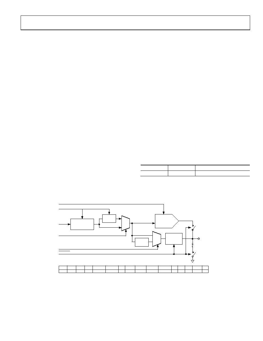
Table 6. Control Register Bits
D15
D14
D13 to D0
0
Control bits
SIN
ROM
PHASE
ACCUMULATOR
(28-BIT)
(LOW POWER)
10-BIT DAC
0
MUX
1
SLEEP12
SLEEP1
RESET
MODE + OPBITEN
DIV2
OPBITEN
VOUT
1
MUX
0
DIGITAL
OUTPUT
(ENABLE)
DIVIDE
BY 2
D15
0
D14
0
D13
B28
D12
HLB
D11
FSEL
D10
PSEL
D9
0
D8
RESET
D7
SLEEP1
D6
SLEEP12
D5
OPBITEN
D4
0
D3
DIV2
D2
0
D1
MODE
D0
0
09070-
024
Figure 20. Function of Control Bits
相关PDF资料 |
PDF描述 |
|---|---|
| V150C36E150BG | CONVERTER MOD DC/DC 36V 150W |
| 4-830611-8 | CONN LEAD ASSY LGH SL END 16 AWG |
| H3CCH-3036M | IDC CABLE - HKC30H/AE30M/HKC30H |
| VE-B6B-EW | CONVERTER MOD DC/DC 95V 100W |
| V150C36E150B | CONVERTER MOD DC/DC 36V 150W |
相关代理商/技术参数 |
参数描述 |
|---|---|
| EVAL-AD9838SDZ | 功能描述:BOARD EVAL FOR AD9838 RoHS:是 类别:编程器,开发系统 >> 评估演示板和套件 系列:- 标准包装:1 系列:- 主要目的:电信,线路接口单元(LIU) 嵌入式:- 已用 IC / 零件:IDT82V2081 主要属性:T1/J1/E1 LIU 次要属性:- 已供物品:板,电源,线缆,CD 其它名称:82EBV2081 |
| EVAL-AD9880-ABZ | 功能描述:KIT MODULE VIDEO INPUT AD9880 RoHS:是 类别:编程器,开发系统 >> 评估演示板和套件 系列:- 标准包装:1 系列:PCI Express® (PCIe) 主要目的:接口,收发器,PCI Express 嵌入式:- 已用 IC / 零件:DS80PCI800 主要属性:- 次要属性:- 已供物品:板 |
| EVAL-ADAS1000EBZU1 | 功能描述:EVAL BOARD ADAS1000 ECG AFE RoHS:是 类别:编程器,开发系统 >> 评估演示板和套件 系列:* 产品培训模块:Obsolescence Mitigation Program 标准包装:1 系列:- 主要目的:电源管理,电池充电器 嵌入式:否 已用 IC / 零件:MAX8903A 主要属性:1 芯锂离子电池 次要属性:状态 LED 已供物品:板 |
| EVAL-ADAS1000SDZ | 功能描述:数据转换 IC 开发工具 EVALUATION BOARD RoHS:否 制造商:Texas Instruments 产品:Demonstration Kits 类型:ADC 工具用于评估:ADS130E08 接口类型:SPI 工作电源电压:- 6 V to + 6 V |
| EVAL-ADAS1000SDZU3 | 制造商:Analog Devices 功能描述:EVALUATION KIT - Boxed Product (Development Kits) |
发布紧急采购,3分钟左右您将得到回复。