- 您现在的位置:买卖IC网 > PDF目录16586 > EVAL-ADCMP603BCPZ (Analog Devices Inc)BOARD EVAL FOR ADCMP603 PDF资料下载
参数资料
| 型号: | EVAL-ADCMP603BCPZ |
| 厂商: | Analog Devices Inc |
| 文件页数: | 4/16页 |
| 文件大小: | 0K |
| 描述: | BOARD EVAL FOR ADCMP603 |
| 标准包装: | 1 |
| 系列: | * |
ADCMP603
Rev. 0 | Page 12 of 16
05
91
5-
02
6
50
150
250
350
450
550
650
H
YST
ER
E
SI
S
(
m
V
)
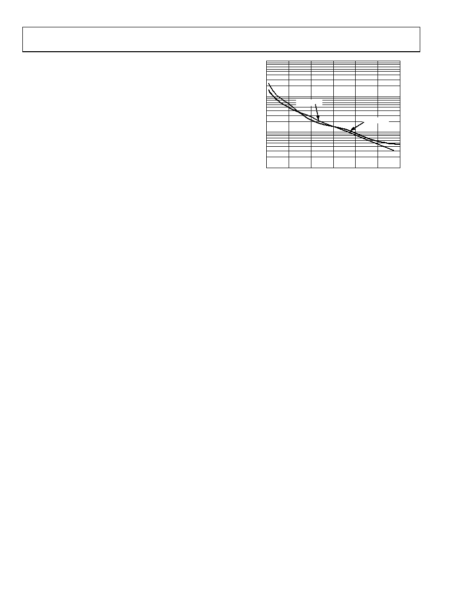
HYSTERESIS RESISTOR (k)
1
10
100
1000
VCC = 5.5V
VCC = 2.5V
The ADCMP603 comparator offers a programmable hysteresis
feature that can significantly improve accuracy and stability.
Connecting an external pull-down resistor or a current source
from the LE/HYS pin to GND varies the amount of hysteresis in
a predictable, stable manner. Leaving the LE/HYS pin
disconnected or driving it high removes the hysteresis. The
maximum hysteresis that can be applied using this pin is
approximately 160 mV. Figure 18 illustrates the amount of
hysteresis applied as a function of the external resistor value,
and Figure 9 illustrates hysteresis as a function of the current.
The hysteresis control pin appears as a 1.25 V bias voltage seen
through a series resistance of 7 kΩ ± 20% throughout the hysteresis
control range. The advantages of applying hysteresis in this manner
are improved accuracy, improved stability, reduced component
count, and maximum versatility. An external bypass capacitor is
not recommended on the HYS pin because it impairs the latch
function and often degrades the jitter performance of the device.
As described in the Using/Disabling the Latch Feature section,
hysteresis control need not compromise the latch function.
Figure 18. Hysteresis vs. R
Control Resistor
HYS
MINIMUM INPUT SLEW RATE REQUIREMENT
With the rated load capacitance and normal good PC Board
design practice, as discussed in the Optimizing Performance
section, these comparators should be stable at any input slew
rate with no hysteresis. Broadband noise from the input stage is
observed in place of the violent chattering seen with most other
high speed comparators. With additional capacitive loading or
poor bypassing, more persistent oscillations are seen. This
oscillation is due to the high gain bandwidth of the comparator
in combination with feedback parasitics in the package and PC
board. In many applications, chattering is not harmful since the
first cycle of the oscillation occurs close to V
CROSSOVER BIAS POINT
In both op amps and comparators, rail-to-rail inputs of this type
have a dual front-end design. Certain devices are active near the
VCC rail and others are active near the VEE rail. At some predeter-
mined point in the common-mode range, a crossover occurs. At
this point, typically VCC/2, the direction of the bias current reverses
and the measured offset voltages and currents change.
OS
.
The ADCMP603 slightly elaborates on this scheme. Crossover
points can be found at approximately 0.8 V and 1.6 V.
相关PDF资料 |
PDF描述 |
|---|---|
| GSM10DRMN | CONN EDGECARD 20POS .156 WW |
| V300B3V3E100BF | CONVERTER MOD DC/DC 3.3V 100W |
| H3DDH-6406M | IDC CABLE - HKR64H/AE64M/HKR64H |
| EEM44DRUI | CONN EDGECARD 88POS DIP .156 SLD |
| V300B3V3E100B3 | CONVERTER MOD DC/DC 3.3V 100W |
相关代理商/技术参数 |
参数描述 |
|---|---|
| EVAL-ADCMP604BKSZ | 功能描述:BOARD EVAL FOR ADCMP604 SC70-6 RoHS:是 类别:编程器,开发系统 >> 评估演示板和套件 系列:- 标准包装:1 系列:- 主要目的:电信,线路接口单元(LIU) 嵌入式:- 已用 IC / 零件:IDT82V2081 主要属性:T1/J1/E1 LIU 次要属性:- 已供物品:板,电源,线缆,CD 其它名称:82EBV2081 |
| EVAL-ADCMP605BCPZ | 功能描述:BOARD EVAL FOR ADCMP605 RoHS:是 类别:编程器,开发系统 >> 评估演示板和套件 系列:- 标准包装:1 系列:- 主要目的:电信,线路接口单元(LIU) 嵌入式:- 已用 IC / 零件:IDT82V2081 主要属性:T1/J1/E1 LIU 次要属性:- 已供物品:板,电源,线缆,CD 其它名称:82EBV2081 |
| EVAL-ADCMP605BCPZ1 | 制造商:AD 制造商全称:Analog Devices 功能描述:Rail-to-Rail, Very Fast, 2.5 V to 5.5 V, Single-Supply LVDS Comparators |
| EVAL-ADCMP606BKSZ | 功能描述:BOARD EVAL FOR ADCMP606 RoHS:是 类别:编程器,开发系统 >> 评估演示板和套件 系列:* 标准包装:1 系列:- 主要目的:电信,线路接口单元(LIU) 嵌入式:- 已用 IC / 零件:IDT82V2081 主要属性:T1/J1/E1 LIU 次要属性:- 已供物品:板,电源,线缆,CD 其它名称:82EBV2081 |
| EVAL-ADCMP607BCPZ | 功能描述:BOARD EVAL FOR ADCMP607 12LFCSP RoHS:是 类别:编程器,开发系统 >> 评估演示板和套件 系列:- 标准包装:1 系列:- 主要目的:电信,线路接口单元(LIU) 嵌入式:- 已用 IC / 零件:IDT82V2081 主要属性:T1/J1/E1 LIU 次要属性:- 已供物品:板,电源,线缆,CD 其它名称:82EBV2081 |
发布紧急采购,3分钟左右您将得到回复。