参数资料
| 型号: | EVDN414 |
| 厂商: | IXYS |
| 文件页数: | 1/2页 |
| 文件大小: | 0K |
| 描述: | BOARD EVALUATION IXDN414 |
| 标准包装: | 1 |
| 主要目的: | 电源管理,FET 驱动器(外部 FET) |
| 已用 IC / 零件: | IXDN414 |
| 已供物品: | 板 |
| 相关产品: | IXDN414YI-ND - IC DRIVER MOSF/IGBT 14A 5-TO-263 IXDN414PI-ND - IC DRIVER MOSF/IGBT 14A 8-DIP IXDN414CI-ND - IC DRIVER MOSF/IGBT 14A TO-220-5 IXDN414SI-ND - IC DRIVER MOSF/IGBT 14A14SOIC |
�� �
�
�EVDD408,� EVDD409,� EVDI409,� EVDN409� And� EVDD414�
�IXDD408,� IXDD409,� IXDI409,� IXDN409� And� IXDD414�
�General� Description�
�Gate� Driver� IC� Evaluation� Boards�
�The� EVDD408/EVDD409/EVDI409/EVDN409/EVDD414�
�evaluation� boards� are� general-purpose� circuit� boards�
�designed� to� simplify� the� evaluation� of� the� IXYS� IXDD408,�
�IXDD409,� IXDI409,� IXDN409� and� IXDD414� gate� drive� ICs,� as�
�well� as� to� provide� a� building� block� for� power� circuit�
�development.� Any� of� the� four� gate� driver� package� types� (SO-�
�8,� Dip� 8,� 5pin� TO-220� and� the� 5pin� TO-263)� may� be� installed�
�in� the� driver� (the� 5-Pin� TO-263� is� factory� installed).� The� board�
�enables� the� user� to� drive� MOSFETs� or� IGBTs� in� the� TO-220,�
�TO-247,� TO-264� or� SOT-227� packages.� The� evaluation�
�board� design� allows� these� MOSFETS� to� be� attached� to� a�
�heat� sink,� and� in� so� doing� the� board� assembly� can� be� used�
�as� a� ground� referenced,� low� side� power� switch� for� both�
�single-ended� and� push-pull� configurations.� The� board� layout�
�for� the� gate� driver� in� the� TO-220� and� the� TO-263� packages�
�(designator� U1B),� allows� the� ground� tab� to� be� soldered� to�
�the� ground� plane� for� cooling� in� high-power,� high� frequency�
�applications� with� large� MOSFET� devices.� Circuitry� for� the� Tri-�
�State� function� is� also� included� on� the� evaluation� board.�
�There� are� three� test� points� on� the� board:� Control,� Gate� and�
�Drain.� These� allow� the� user� to� easily� attach� an� oscilloscope�
�probe� and� the� associated� ground� to� the� circuit� to� verify�
�performance.�
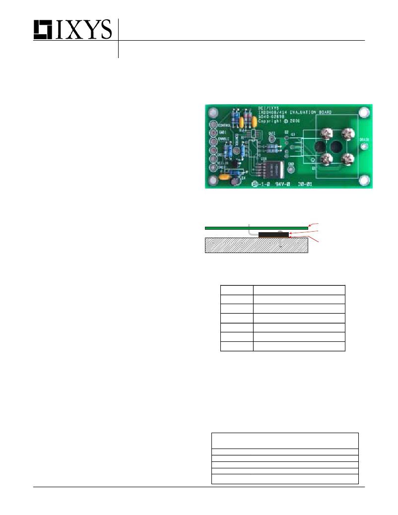
�Figure� 1� -� EVDD408/EVDD409/EVDI409/EVDN409/EVDD414�
�Evaluation� Board�
�SOT-227� Device� Installed� For� Illustration� Purposes� Only�
�Figure� 1� is� a� photograph� of� the� Evaluation� Board� loaded� with�
�an� IXDD408YI� TO-263� driver� and� a� SOT-227� MOSFET.� The�
�low� level� inputs� are� shown� on� the� left� side� of� the� board.�
�Evaluation� PCB�
�Control� is� a� TTL� high� true� input� which� controls� the� on� or� off�
�state� of� the� power� switch� Q1,� Q2,� or� Q3.� Enable� is� a� low� true�
�input,� which� controls� the� Tri-State� output� (IXDD408,� IXDD409�
�and� IXDD414� devices� only).� VCC-IN� is� the� low� voltage,� (8-�
�Heat� Sink�
�TO-220,� TO-247,�
�TO-264,� or� SOT-227�
�Kapton� Insulator�
�25V)� power� input,� (see� Figure� 3� below).� Figure� 2� illustrates�
�the� MOSFET� mounting� of� a� TO-220,� TO-247,� or� TO-264�
�device.� The� MOSFET� is� mounted� on� the� back� side� of� the�
�PCB.� A� large� through� hole� is� provided� so� that� the� device� can�
�Figure� 2� -� Evaluation� Board� Side� View� Showing� Power�
�Device� Installed� In� A� High-Power� Configuration�
�be� attached� to� a� heat� sink.� The� SOT-227� (shown� in� the�
�photograph)� is� mounted� in� a� similar� manner.�
�Circuit� Operation�
�The� schematic� diagram� for� the� evaluation� board� is� shown� in�
�Figure� 4.� The� control� gate� is� applied� to� R6� then� on� the� input�
�pin� 2� of� the� IC.� This� signal� input� is� followed� in� time� by� the�
�output� pins� 7� and� 6.� Pins� 1� and� 8� are� attached� to� +VCC� via� a�
�de-coupling� network� comprised� of� R1,� C1� and� R2,� C2.� Pins�
�INPUT�
�CONTROL�
�GND1�
�ENABLE� *�
�GND2�
�VCC-IN�
�GND� 3�
�FUNCTION�
�Control� Input� -� 3V� into� 1K� Ohms�
�Ground� 1�
�LOW� =� True,� HIGH� =� Tri-State� Mode�
�Ground� 2�
�VCC� input� -� 8V� to� 25V�
�Ground� 3�
�4� and� 5� are� attached� to� the� circuit� ground� plane.� This� is� the�
�preferred� arrangement� of� the� bypassing� for� the� Vcc� input�
�power.� The� enable� pin� 3� is� attached� to� the� drain� of� Q4.� This�
�device� is� used� to� level� translate� and� provide� an� invert�
�function� for� the� Tri-State� mode� when� used� with� the� IXDD408,�
�IXDD409� and� IXDD414� devices.� (The� IXDI409� and� IXDN409�
�devices� do� not� utilize� the� enable� input.)� The� drain� of� Q4� is�
�also� attached� to� the� gate� of� the� MOSFET� thru� RA� and� DA.� In�
�the� Tri-State� mode� the� turn-off� time� of� the� power� MOSFET� is�
�determined� by� the� time� constant� of� the� input� gate�
�capacitance� C� iss� and� the� value� of� the� resistor� RA.� See� the�
�IXDD408� and� IXDD414� data� sheets� for� additional�
�information� on� this� mode� of� operation.�
�*� Enable� function� applies� to� IXDD408,� IXDD409� and�
�IXDD414� devices� only�
�Figure� 3� -� Input� Pin-Out� Table�
�The� Evaluation� Boards� are� supplied� with� either� IXDD408YI,�
�IXDD409YI,� IXDI409YI,� IXDN409YI� or� IXDD414YI� 5-Pin� TO-�
�263� devices� installed,� depending� upon� the� evaluation� baord�
�part� number� ordered.� To� use� the� evaluation� board� with� a�
�different� package� type,� the� installed� device� must� be� re-�
�moved,� and� the� new� device� installed� in� the� appropriate�
�location.�
�Ordering� Information�
�The� U1� output� is� available� at� pins� 7� and� 6.� These� are�
�attached� to� the� MOSFET� via� the� two� one-Ohm� resistors� R4�
�and� R5.� The� values� of� these� resistors� may� be� changed� to�
�optimize� the� performance� of� the� specific� device� being� driven.�
�Part� Number�
�EVDD408�
�EVDD409�
�EVDI409�
�EVDN409�
�EVDD414�
�Installed� Device�
�IXDD408YI� 5-Pin� TO-263,� 8A� With� Enable�
�IXDD409YI� 5-Pin� TO-263,� 9A� With� Enable�
�IXDI409YI� 5-Pin� TO-263,� 9A� Inverting�
�IXDN409YI 5-Pin TO-263, 9A Non-Inverting�
�IXDD414YI� 5-Pin� TO-263,� 14A� With� Enable�
�Copyright� ?� IXYS� CORPORATION� 2001,� 2002�
�First� Release�
�相关PDF资料 |
PDF描述 |
|---|---|
| EVDP610 | BOARD EVALUATION IXDP610 |
| EYP-2MT098B | THERMAL CUTOFF 98C 2A/50VDC TAB |
| EZ3-A230XF1 | SURGE ARRESTER 230V GASTUBE 3PIN |
| EZJ-Z1V39010 | VARISTOR MULTILAYER 39V 0603 |
| EZN-4100LCMUS-2 | KEYBOARD EZCLEAN 83 KEYS USB |
相关代理商/技术参数 |
参数描述 |
|---|---|
| EVDN430CI | 功能描述:电源管理IC开发工具 30A Ultra Fast MOSFET/IGBT Driver RoHS:否 制造商:Maxim Integrated 产品:Evaluation Kits 类型:Battery Management 工具用于评估:MAX17710GB 输入电压: 输出电压:1.8 V |
| EVDN430MCI | 功能描述:电源管理IC开发工具 30A Ultra Fast MOSFET/IGBT Driver RoHS:否 制造商:Maxim Integrated 产品:Evaluation Kits 类型:Battery Management 工具用于评估:MAX17710GB 输入电压: 输出电压:1.8 V |
| EVDN430MYI | 功能描述:电源管理IC开发工具 30A Ultra Fast MOSFET/IGBT Driver RoHS:否 制造商:Maxim Integrated 产品:Evaluation Kits 类型:Battery Management 工具用于评估:MAX17710GB 输入电压: 输出电压:1.8 V |
| EVDN430YI | 功能描述:电源管理IC开发工具 30A Ultra Fast MOSFET/IGBT Driver RoHS:否 制造商:Maxim Integrated 产品:Evaluation Kits 类型:Battery Management 工具用于评估:MAX17710GB 输入电压: 输出电压:1.8 V |
| EVDO910CF V3.0 | 制造商:Janus Remote Communications 功能描述:TERMINUS PLUG-IN SERIES GSM865CF TERMINAL MODEM |
发布紧急采购,3分钟左右您将得到回复。