参数资料
| 型号: | EX256-TQ100A |
| 厂商: | Microsemi SoC |
| 文件页数: | 24/48页 |
| 文件大小: | 0K |
| 描述: | IC FPGA ANTIFUSE 12K 100-TQFP |
| 标准包装: | 90 |
| 系列: | EX |
| 逻辑元件/单元数: | 512 |
| 输入/输出数: | 81 |
| 门数: | 12000 |
| 电源电压: | 2.3 V ~ 2.7 V |
| 安装类型: | 表面贴装 |
| 工作温度: | -40°C ~ 125°C |
| 封装/外壳: | 100-LQFP |
| 供应商设备封装: | 100-TQFP(14x14) |
第1页第2页第3页第4页第5页第6页第7页第8页第9页第10页第11页第12页第13页第14页第15页第16页第17页第18页第19页第20页第21页第22页第23页当前第24页第25页第26页第27页第28页第29页第30页第31页第32页第33页第34页第35页第36页第37页第38页第39页第40页第41页第42页第43页第44页第45页第46页第47页第48页
eX FPGA Architecture and Characteristics
1-26
Revision 10
Timing Characteristics
Timing characteristics for eX devices fall into three categories: family-dependent, device-dependent, and
design-dependent. The input and output buffer characteristics are common to all eX family members.
Internal routing delays are device-dependent. Design dependency means actual delays are not
determined until after placement and routing of the user’s design are complete. Delay values may then
be determined by using the Timer utility or performing simulation with post-layout delays.
Critical Nets and Typical Nets
Propagation delays are expressed only for typical nets, which are used for initial design performance
evaluation. Critical net delays can then be applied to the most timing critical paths. Critical nets are
determined by net property assignment prior to placement and routing. Up to six percent of the nets in a
design may be designated as critical.
Long Tracks
Some nets in the design use long tracks. Long tracks are special routing resources that span multiple
rows, columns, or modules. Long tracks employ three to five antifuse connections. This increases
capacitance and resistance, resulting in longer net delays for macros connected to long tracks. Typically,
no more than six percent of nets in a fully utilized device require long tracks. Long tracks contribute
approximately 4 ns to 8.4 ns delay. This additional delay is represented statistically in higher fanout
routing delays.
Timing Derating
eX devices are manufactured with a CMOS process. Therefore, device performance varies according to
temperature, voltage, and process changes. Minimum timing parameters reflect maximum operating
voltage, minimum operating temperature, and best-case processing. Maximum timing parameters reflect
minimum operating voltage, maximum operating temperature, and worst-case processing.
Temperature and Voltage Derating Factors
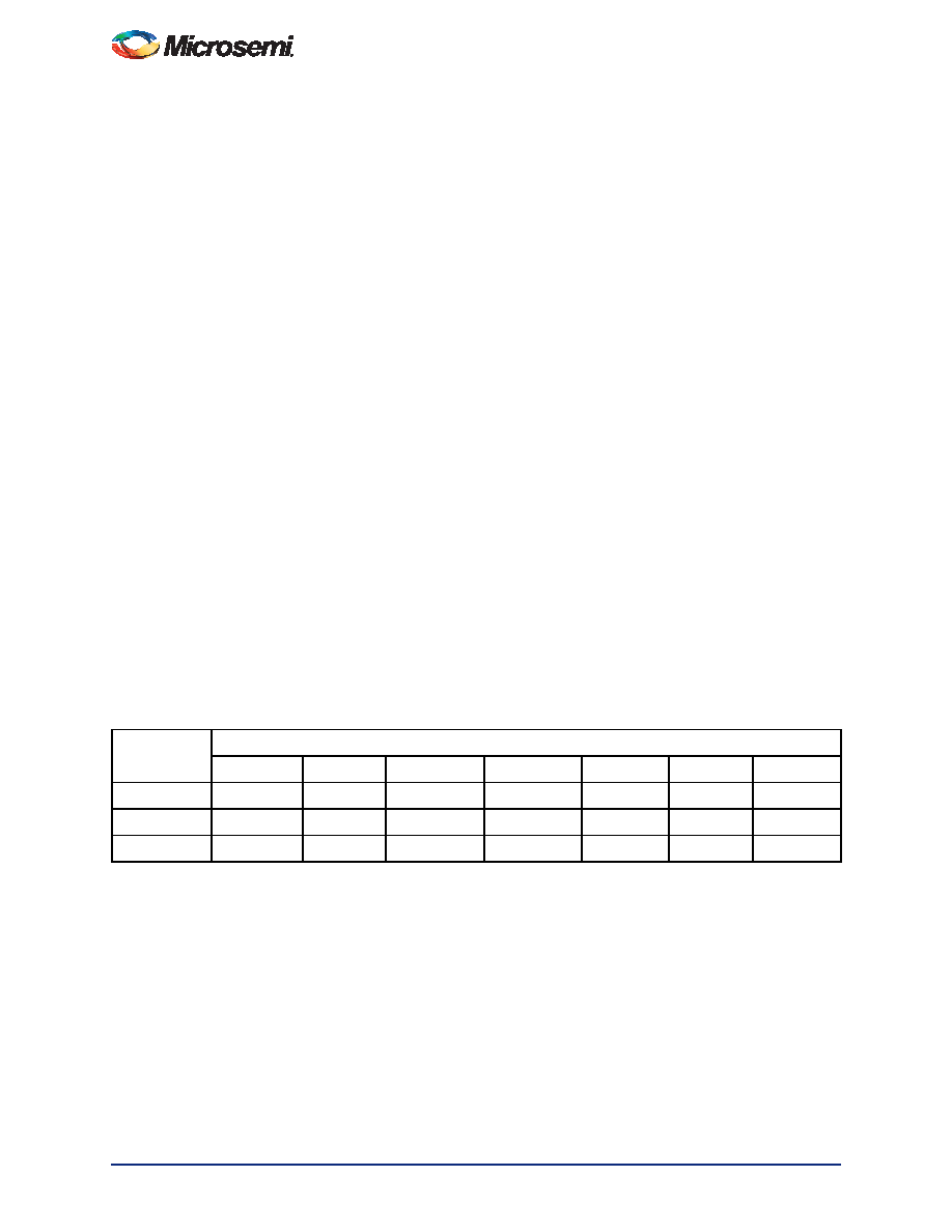
Table 1-16 Temperature and Voltage Derating Factors
(Normalized to Worst-Case Commercial, TJ = 70C, VCCA = 2.3V)
VCCA
Junction Temperature (TJ)
–55
–40
0
25
70
85
125
2.3
0.79
0.80
0.87
0.88
1.00
1.04
1.13
2.5
0.74
0.81
0.83
0.93
0.97
1.06
2.7
0.69
0.70
0.76
0.78
0.88
0.91
1.00
相关PDF资料 |
PDF描述 |
|---|---|
| EX256-TQG100A | IC FPGA ANTIFUSE 12K 100-TQFP |
| EP4CE10E22I8L | IC CYCLONE IV FPGA 10K 144EQFP |
| EP4CE10E22I7 | IC CYCLONE IV FPGA 10K 144EQFP |
| EP4CE10E22C6 | IC CYCLONE IV FPGA 10K 144EQFP |
| EP4CE10F17C8L | IC CYCLONE IV FPGA 10K 256FBGA |
相关代理商/技术参数 |
参数描述 |
|---|---|
| EX256-TQ100I | 功能描述:IC FPGA ANTIFUSE 12K 100-TQFP RoHS:否 类别:集成电路 (IC) >> 嵌入式 - FPGA(现场可编程门阵列) 系列:EX 标准包装:90 系列:ProASIC3 LAB/CLB数:- 逻辑元件/单元数:- RAM 位总计:36864 输入/输出数:157 门数:250000 电源电压:1.425 V ~ 1.575 V 安装类型:表面贴装 工作温度:-40°C ~ 125°C 封装/外壳:256-LBGA 供应商设备封装:256-FPBGA(17x17) |
| EX256-TQ100PP | 制造商:ACTEL 制造商全称:Actel Corporation 功能描述:eX Family FPGAs |
| EX256-TQG100 | 功能描述:IC FPGA ANTIFUSE 12K 100-TQFP RoHS:是 类别:集成电路 (IC) >> 嵌入式 - FPGA(现场可编程门阵列) 系列:EX 标准包装:152 系列:IGLOO PLUS LAB/CLB数:- 逻辑元件/单元数:792 RAM 位总计:- 输入/输出数:120 门数:30000 电源电压:1.14 V ~ 1.575 V 安装类型:表面贴装 工作温度:-40°C ~ 85°C 封装/外壳:289-TFBGA,CSBGA 供应商设备封装:289-CSP(14x14) |
| EX256-TQG100A | 功能描述:IC FPGA ANTIFUSE 12K 100-TQFP RoHS:是 类别:集成电路 (IC) >> 嵌入式 - FPGA(现场可编程门阵列) 系列:EX 标准包装:152 系列:IGLOO PLUS LAB/CLB数:- 逻辑元件/单元数:792 RAM 位总计:- 输入/输出数:120 门数:30000 电源电压:1.14 V ~ 1.575 V 安装类型:表面贴装 工作温度:-40°C ~ 85°C 封装/外壳:289-TFBGA,CSBGA 供应商设备封装:289-CSP(14x14) |
| EX256-TQG100I | 功能描述:IC FPGA ANTIFUSE 12K 100-TQFP RoHS:是 类别:集成电路 (IC) >> 嵌入式 - FPGA(现场可编程门阵列) 系列:EX 标准包装:90 系列:ProASIC3 LAB/CLB数:- 逻辑元件/单元数:- RAM 位总计:36864 输入/输出数:157 门数:250000 电源电压:1.425 V ~ 1.575 V 安装类型:表面贴装 工作温度:-40°C ~ 125°C 封装/外壳:256-LBGA 供应商设备封装:256-FPBGA(17x17) |
发布紧急采购,3分钟左右您将得到回复。