- 您现在的位置:买卖IC网 > PDF目录67411 > FA13843P 1 A SWITCHING CONTROLLER, 57 kHz SWITCHING FREQ-MAX, PDIP8 PDF资料下载
参数资料
| 型号: | FA13843P |
| 元件分类: | 稳压器 |
| 英文描述: | 1 A SWITCHING CONTROLLER, 57 kHz SWITCHING FREQ-MAX, PDIP8 |
| 封装: | DIP-8 |
| 文件页数: | 15/15页 |
| 文件大小: | 151K |
| 代理商: | FA13843P |
FA13842, 13843, 13844, 13845
9
5. Output stage
An output stage of CMOS inverter composition is incorporated,
thereby making it possible to fully swing the gate voltage of a
power MOSFET to the VCC.
The output stage provides a source current of 400mA and a
sink current of 1A as the peak current capacity. (When VCC is
15V)
The output stage is held in the “Low” state in standby mode.
6. Reference voltage
The 5.0V(
±5%) bandgap reference(Tj=25C) is built-in.
It is possible to supply a current of about 10mA to an external
circuit in addition to supplying a charge current to the timing
capacitor of the oscillator. (See characteristic curve on page
46.)
Connect a ceramic bypass capacitor of 0.1
F or higher to the
VREF terminal to stabilize this voltage.
s Design advice
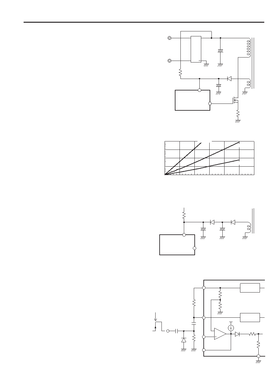
1. Start-up circuit
A typical start-up circuit is shown in Fig. 4.
The AC INPUT voltage charges capacitor C2 and supplies
start-up current to the IC through start-up resistance R1. When
this voltage reaches the ON threshold voltage, the IC reverts to
the operation mode and electric power is supplied from the
bias winding of the transformer thereafter.
Using CMOS process, the start-up current is less than 30
A.
When the start-up resistance is increased, the charging rate of
capacitor C2 decreases and start-up time increases. Select
the optimum values for R1 and C2.
The relation between the start-up resistance and start-up time
for the circuit indicated in Fig. 4 is shown in Fig. 5.
Fig. 6 indicates a method to increase the start-up resistance to
reduce loss and shorten start-up time. The start-up time is
shortened by reducing the capacitance of C2. The bias current
is supplied from C3 after start-up.
2. Synchronized operation with external signals
The circuit shown in Fig. 7 allows synchronized operation with
external signals.
Synchronized operation is started when the RT/CT terminal
voltage is raised to about 3V or higher. (Synchronized at
leading edge.)
The external synchronizing signal should be higher than the
free-run frequency.
In the case of FA13844/45, the output frequency of the OUT
terminal is 1/2 that of the synchronizing signal frequency.
Fig. 5
Start-up time
4
3
2
Start-up
time[sec]
1
0
200
400
600
Start-up resistance R1 (k
)
C2=47
F
C2=10
F
800
1000
1200
C2=22
F
Input:100V AC
Fig. 7
+
D3
R2
ER AMP
2R
1R
Synchronized
C4
OSC
REF
5
1
2
4
RT
CT
8
~+
~
DB
R1
D1
C2
MOSFET
Rs
6
7
FA13842
+
C1
T1
AC INPUT
+
Fig. 4
Fig. 6
D2
R1
D1
C2
FA13842
+
C3
+
6
7
相关PDF资料 |
PDF描述 |
|---|---|
| FA13842N | 1 A SWITCHING CONTROLLER, 57 kHz SWITCHING FREQ-MAX, PDSO8 |
| FA13843N | 1 A SWITCHING CONTROLLER, 57 kHz SWITCHING FREQ-MAX, PDSO8 |
| FA13844N | 1 A SWITCHING CONTROLLER, 57 kHz SWITCHING FREQ-MAX, PDSO8 |
| FA13845N | 1 A SWITCHING CONTROLLER, 57 kHz SWITCHING FREQ-MAX, PDSO8 |
| FA13842P | 1 A SWITCHING CONTROLLER, 57 kHz SWITCHING FREQ-MAX, PDIP8 |
相关代理商/技术参数 |
参数描述 |
|---|---|
| FA13843P-D1 | 制造商:Fuji Electric 功能描述: |
| FA13844 | 制造商:未知厂家 制造商全称:未知厂家 功能描述:电源电路,类似UA3843 |
| FA13844N | 制造商:Panasonic Industrial Company 功能描述:IC |
| FA13844N-TE1 | 制造商:FUJI 制造商全称:Fuji Electric 功能描述:CURRENT MODE PWM CONTROLLER |
| FA13844P | 制造商:FUJI 制造商全称:Fuji Electric 功能描述:CMOS IC(For Switching Power Supply Control) |
发布紧急采购,3分钟左右您将得到回复。